Altera® FPGA and SoC FPGA
Altera® FPGAs offer a wide variety of configurable embedded SRAM, high-speed transceivers, high-speed I/Os, logic blocks, and routing. Built-in intellectual property (IP) combined with outstanding software tools lower FPGA development time, power, and cost.
Altera® FPGA and SoC FPGA
Extended product longevity mitigates the risk of obsolescence and minimizes the cost of redesigning. Therefore, our customers can have peace of mind choosing our products and continue to rely on our widely used FPGAs and CPLDs with confidence. Altera device availability now extends to:
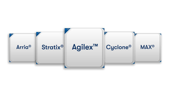
2040: Cyclone® 10 LP, Cyclone® V, Cyclone® IV, Cyclone® III, MAX® 10, MAX® V, MAX® II.1
2035: Agilex™ 7 FPGA F-Series, Agilex™ 7 FPGA I-Series, Stratix® 102, Stratix® V, Stratix® IV, Stratix® III, Arria® 10, Arria® V, Arria® II, Cyclone 10® GX, Cyclone® II.1
Resources to Help You Get Started Today
FPGA Design Software, Tools, Quartus® Prime Software
Browse the complete suite of development tools for every stage of your design.
FPGA Intellectual Property
Browse our IP portfolio for a wide variety of applications.
FPGA Development Kits
Browse our selection of development kits to accelerate your FPGA design process.
FPGA Acceleration Platforms and System-on-Modules (SoMs)
Learn more about our FPGA acceleration platforms, including SmartNICs, Infrastructure Processing Units (IPUs), and SoMs.
Download FPGA Product Catalog
Our SoC FPGA Ecosystem
Our SoC FPGAs are ARM processor-based and inherit the strength of its ecosystem.
More FPGA Support Resources
Check out other resources to learn how to use/design with FPGAs.
FAQs
Frequently Asked Questions
FPGA or field programmable gate array is a semiconductor integrated circuit with customized electrical functionality to accelerate key workloads.
FPGA is a semiconductor IC where the design engineer can change most of the electrical functionality inside the device during the PCB assembly process or even after the equipment has been shipped to customers out in the ‘field.’
SoC FPGA devices integrate both processor and FPGA architectures into a single device.
Integrating the high-level management functionality of processors and the stringent, real-time operations, extreme data processing, or interface functions of an FPGA (Field Programmable Gate Array) into a single device forms an even more powerful embedded computing platform.
Consequently, they provide higher integration, lower power, small board size, and higher bandwidth communication between the processor and FPGA. They also include a rich set of peripherals, on-chip memory, an FPGA-style logic array, and high-speed transceivers.
Flexibility
FPGA functionality can change upon every power-up of the device.
Acceleration
Get products to market quickly and increase your system performance.
Integration
Today’s FPGAs include chiplet-based heterogenous integration, on-die processors, transceivers, RAM blocks, digital signal processor (DSP) engines, and more.
Total Cost of Ownership (TCO)
While ASICs may cost less per unit than an equivalent FPGA, building them requires a non-recurring expense (NRE), expensive software tools, specialized design teams, and long manufacturing cycles.

Subscribe to our FPGA Newsletter
Get the latest information about FPGAs, programmable accelerators, development flows, solutions, training, and tools.
Product and Performance Information
Unforeseen supply disruptions such as vendor discontinuance, change in government regulations, or production tools obsolescence may impact Altera’s ability to offer the products.
Excluding Stratix 10 with HBM2 memory.