1.8. Appendix
Quartus Tool Version
Intel® Quartus® Prime Pro Edition software version 17.0IR2 Build 116 (with patch version 0.02IR2) is used for compilation of designs.
Core PLL
Intel® Stratix® 10 fPLL is used as core PLL in the design to generate link and frame clocks from the reference clock received from converter.
SYSREF Detection
Continuous SYSREF detection mode is enabled on ADC. Without continuous sysref detection on ADC side few modes exhibit variable link latency. The modes that exhibit variable link latency are LMF = 118, 214, and 412. For uniformity, all the JESD configurations are enabled with continuous SYSREF generation.
DDC Enable Modes
Figure 7 shows the JESD configurations supported by the ADC. The highlighted rows in the table are the configurations that are implemented in reference designs.
Figure 7. JESD204B Mode of Operation (M = 1, S = 4, N' = 16, Unless Otherwise Noted)
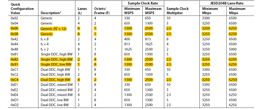
The criteria for selection of mode was the sampling rate of ADC. Note that the maximum sampling rate for all the selected JESD configurations in the table is 2500 MSPS. The AD9625 EVMhas a fixed oscillator of 2500 MHz (also highlighted in Figure 2. This oscillator generates the ADC sampling clock. As a result, the ADC sampling rate is always fixed to 2500 Msps.
This was the rationale behind selection of JESD modes. It is observed that modes with 1, 2, and 4 lanes have DDC enabled.
JESD Lane Rate Selection
As explained in previous section, the ADC sampling rate is fixed to 2500 Msps. This also restricts the flexibility to change JESD lane rates. In all the variants, the maximum JESD lane rate achievable is 6250 Mbps.