Visible to Intel only — GUID: bbd1547062670756
Ixiasoft
1. About the External Memory Interfaces Agilex™ 7 F-Series and I-Series FPGA IP
2. Agilex™ 7 F-Series and I-Series FPGA EMIF IP – Introduction
3. Agilex™ 7 F-Series and I-Series FPGA EMIF IP – Product Architecture
4. Agilex™ 7 F-Series and I-Series FPGA EMIF IP – End-User Signals
5. Agilex™ 7 F-Series and I-Series FPGA EMIF IP – Simulating Memory IP
6. Agilex™ 7 F-Series and I-Series FPGA EMIF IP – DDR4 Support
7. Agilex™ 7 F-Series and I-Series FPGA EMIF IP – QDR-IV Support
8. Agilex™ 7 F-Series and I-Series FPGA EMIF IP – Timing Closure
9. Agilex™ 7 F-Series and I-Series FPGA EMIF IP – I/O Timing Closure
10. Agilex™ 7 F-Series and I-Series FPGA EMIF IP – Controller Optimization
11. Agilex™ 7 F-Series and I-Series FPGA EMIF IP – Debugging
12. External Memory Interfaces Agilex™ 7 F-Series and I-Series FPGA IP User Guide Archives
13. Document Revision History for External Memory Interfaces Agilex™ 7 F-Series and I-Series FPGA IP User Guide
3.1. Intel® Agilex™ 7 F-Series and I-Series EMIF Architecture: Introduction
3.2. Intel® Agilex™ 7 F-Series and I-Series EMIF Sequencer
3.3. Intel® Agilex™ 7 F-Series and I-Series EMIF Calibration
3.4. Intel® Agilex™ 7 F-Series and I-Series EMIF Controller
3.5. User-requested Reset in Intel® Agilex™ 7 F-Series and I-Series EMIF IP
3.6. Intel® Agilex™ 7 F-Series and I-Series EMIF for Hard Processor Subsystem
3.7. Using a Custom Controller with the Hard PHY
3.1.1. Intel® Agilex™ 7 F-Series and I-Series EMIF Architecture: I/O Subsystem
3.1.2. Intel® Agilex™ 7 F-Series and I-Series EMIF Architecture: I/O SSM
3.1.3. Intel® Agilex™ 7 F-Series and I-Series EMIF Architecture: I/O Bank
Zipper Block
I/O Sub-Bank Usage
3.1.4. Intel® Agilex™ 7 F-Series and I-Series EMIF Architecture: I/O Lane
3.1.5. Intel® Agilex™ 7 F-Series and I-Series EMIF Architecture: Input DQS Clock Tree
3.1.6. Intel® Agilex™ 7 F-Series and I-Series EMIF Architecture: PHY Clock Tree
3.1.7. Intel® Agilex™ 7 F-Series and I-Series EMIF Architecture: PLL Reference Clock Networks
3.1.8. Intel® Agilex™ 7 F-Series and I-Series EMIF Architecture: Clock Phase Alignment
3.3.4.3.1. Debugging Calibration Failure Using Information from the Calibration report
3.3.4.3.2. Debugging Address and Command Leveling Calibration Failure
3.3.4.3.3. Debugging Address and Command Deskew Failure
3.3.4.3.4. Debugging DQS Enable Failure
3.3.4.3.5. Debugging Read Deskew Calibration Failure
3.3.4.3.6. Debugging VREFIN Calibration Failure
3.3.4.3.7. Debugging LFIFO Calibration Failure
3.3.4.3.8. Debugging Write Leveling Failure
3.3.4.3.9. Debugging Write Deskew Calibration Failure
3.3.4.3.10. Debugging VREFOUT Calibration Failure
4.1. Intel® Agilex™ 7 F-Series and I-Series EMIF IP Interface and Signal Descriptions
4.2. Intel® Agilex™ 7 F-Series and I-Series EMIF IP AFI Signals
4.3. Intel® Agilex™ 7 F-Series and I-Series EMIF IP AFI 4.0 Timing Diagrams
4.4. Intel® Agilex™ 7 F-Series and I-Series EMIF IP Memory Mapped Register (MMR) Tables
4.1.1.1. local_reset_req for DDR4
4.1.1.2. local_reset_status for DDR4
4.1.1.3. pll_ref_clk for DDR4
4.1.1.4. pll_locked for DDR4
4.1.1.5. ac_parity_err for DDR4
4.1.1.6. oct for DDR4
4.1.1.7. mem for DDR4
4.1.1.8. status for DDR4
4.1.1.9. afi_reset_n for DDR4
4.1.1.10. afi_clk for DDR4
4.1.1.11. afi_half_clk for DDR4
4.1.1.12. afi for DDR4
4.1.1.13. emif_usr_reset_n for DDR4
4.1.1.14. emif_usr_clk for DDR4
4.1.1.15. ctrl_amm for DDR4
4.1.1.16. ctrl_amm_aux for DDR4
4.1.1.17. ctrl_auto_precharge for DDR4
4.1.1.18. ctrl_user_priority for DDR4
4.1.1.19. ctrl_ecc_user_interrupt for DDR4
4.1.1.20. ctrl_ecc_readdataerror for DDR4
4.1.1.21. ctrl_ecc_status for DDR4
4.1.1.22. ctrl_mmr_slave for DDR4
4.1.1.23. hps_emif for DDR4
4.1.1.24. emif_calbus for DDR4
4.1.1.25. emif_calbus_clk for DDR4
4.1.2.1. local_reset_req for QDR-IV
4.1.2.2. local_reset_status for QDR-IV
4.1.2.3. pll_ref_clk for QDR-IV
4.1.2.4. pll_locked for QDR-IV
4.1.2.5. oct for QDR-IV
4.1.2.6. mem for QDR-IV
4.1.2.7. status for QDR-IV
4.1.2.8. afi_reset_n for QDR-IV
4.1.2.9. afi_clk for QDR-IV
4.1.2.10. afi_half_clk for QDR-IV
4.1.2.11. afi for QDR-IV
4.1.2.12. emif_usr_reset_n for QDR-IV
4.1.2.13. emif_usr_clk for QDR-IV
4.1.2.14. ctrl_amm for QDR-IV
4.1.2.15. emif_calbus for QDR-IV
4.1.2.16. emif_calbus_clk for QDR-IV
4.4.1. ctrlcfg0
4.4.2. ctrlcfg1
4.4.3. dramtiming0
4.4.4. sbcfg1
4.4.5. caltiming0
4.4.6. caltiming1
4.4.7. caltiming2
4.4.8. caltiming3
4.4.9. caltiming4
4.4.10. caltiming9
4.4.11. dramaddrw
4.4.12. sideband0
4.4.13. sideband1
4.4.14. sideband4
4.4.15. sideband6
4.4.16. sideband7
4.4.17. sideband9
4.4.18. sideband11
4.4.19. sideband12
4.4.20. sideband13
4.4.21. sideband14
4.4.22. dramsts
4.4.23. niosreserve0
4.4.24. niosreserve1
4.4.25. sideband16
4.4.26. ecc3: ECC Error and Interrupt Configuration
4.4.27. ecc4: Status and Error Information
4.4.28. ecc5: Address of Most Recent SBE/DBE
4.4.29. ecc6: Address of Most Recent Correction Command Dropped
4.4.30. ecc7: Extension for Address of Most Recent SBE/DBE
4.4.31. ecc8: Extension for Address of Most Recent Correction Command Dropped
6.1. Intel® Agilex™ 7 F-Series and I-Series FPGA EMIF IP Parameter Descriptions
6.2. Intel® Agilex™ 7 F-Series and I-Series External Memory Interfaces Intel® Calibration IP Parameters
6.3. Register Map IP-XACT Support for Intel® Agilex™ 7 F-Series and I-Series EMIF DDR4 IP
6.4. Intel® Agilex™ 7 F-Series and I-Series FPGA EMIF IP Pin and Resource Planning
6.5. DDR4 Board Design Guidelines
6.1.1. Intel® Agilex™ 7 F-Series and I-Series EMIF IP DDR4 Parameters: General
6.1.2. Intel® Agilex™ 7 F-Series and I-Series EMIF IP DDR4 Parameters: Memory
6.1.3. Intel® Agilex™ 7 F-Series and I-Series EMIF IP DDR4 Parameters: Mem I/O
6.1.4. Intel® Agilex™ 7 F-Series and I-Series EMIF IP DDR4 Parameters: FPGA I/O
6.1.5. Intel® Agilex™ 7 F-Series and I-Series EMIF IP DDR4 Parameters: Mem Timing
6.1.6. Intel® Agilex™ 7 F-Series and I-Series EMIF IP DDR4 Parameters: Controller
6.1.7. Intel® Agilex™ 7 F-Series and I-Series EMIF IP DDR4 Parameters: Diagnostics
6.1.8. Intel® Agilex™ 7 F-Series and I-Series EMIF IP DDR4 Parameters: Example Designs
6.5.1. Terminations for DDR4 with Intel® Agilex™ 7 F-Series and I-Series Devices
6.5.2. Clamshell Topology
6.5.3. General Layout Routing Guidelines
6.5.4. Reference Stackup
6.5.5. Intel® Agilex™ 7 F-Series and I-Series EMIF-Specific Routing Guidelines for Various DDR4 Topologies
6.5.6. DDR4 Routing Guidelines: Discrete (Component) Topologies
6.5.7. Intel® Agilex™ 7 F-Series and I-Series EMIF Pin Swapping Guidelines
6.5.5.1. One DIMM per Channel (1DPC) for UDIMM, RDIMM, LRDIMM, and SODIMM DDR4 Topologies
6.5.5.2. Two DIMMs per Channel (2DPC) for UDIMM, RDIMM, and LRDIMM DDR4 Topologies
6.5.5.3. Two DIMMs per Channel (2DPC) for SODIMM Topology
6.5.5.4. Skew Matching Guidelines for DIMM Configurations
6.5.5.5. Power Delivery Recommendations for the Memory / DIMM Side
6.5.6.1. Single Rank x 8 Discrete (Component) Topology
6.5.6.2. Single Rank x 16 Discrete (Component) Topology
6.5.6.3. ADDR/CMD Reference Voltage/RESET Signal Routing Guidelines for Single Rank x 8 and R Rank x 16 Discrete (Component) Topologies
6.5.6.4. Skew Matching Guidelines for DDR4 Discrete Configurations
6.5.6.5. Power Delivery Recommendations for DDR4 Discrete Configurations
7.1.1. Intel® Agilex™ 7 F-Series and I-Series EMIF IP QDR-IV Parameters: General
7.1.2. Intel® Agilex™ 7 F-Series and I-Series EMIF IP QDR-IV Parameters: Memory
7.1.3. Intel® Agilex™ 7 F-Series and I-Series EMIF IP QDR-IV Parameters: FPGA I/O
7.1.4. Intel® Agilex™ 7 F-Series and I-Series EMIF IP QDR-IV Parameters: Mem Timing
7.1.5. Intel® Agilex™ 7 F-Series and I-Series EMIF IP QDR-IV Parameters: Controller
7.1.6. Intel® Agilex™ 7 F-Series and I-Series EMIF IP QDR-IV Parameters: Diagnostics
7.1.7. Intel® Agilex™ 7 F-Series and I-Series EMIF IP QDR-IV Parameters: Example Designs
7.3.3.1. Intel® Agilex™ 7 F-Series and I-Series FPGA EMIF IP Banks
7.3.3.2. General Guidelines
7.3.3.3. QDR IV SRAM Commands and Addresses, AP, and AINV Signals
7.3.3.4. QDR IV SRAM Clock Signals
7.3.3.5. QDR IV SRAM Data, DINV, and QVLD Signals
7.3.3.6. Specific Pin Connection Requirements
7.3.3.7. Resource Sharing Guidelines (Multiple Interfaces)
9.1. I/O Timing Closure Overview
9.2. Collateral Generated with Your EMIF IP
9.3. SPICE Decks
9.4. File Organization
9.5. Top-level Parameterization File
9.6. IP-Supplied Parameters that You Might Need to Override
9.7. Understanding the *_ip_parameters.dat File and Making a Mask Polygon
9.8. Multi-Rank Topology
9.9. Pin Parasitics
9.10. Mask Evaluation
10.4.1. Auto-Precharge Commands
10.4.2. Additive Latency
10.4.3. Bank Interleaving
10.4.4. Additive Latency and Bank Interleaving
10.4.5. User-Controlled Refresh
10.4.6. Frequency of Operation
10.4.7. Series of Reads or Writes
10.4.8. Data Reordering
10.4.9. Starvation Control
10.4.10. Command Reordering
10.4.11. Bandwidth
10.4.12. Enable Command Priority Control
10.4.13. Controller Pre-pay and Post-pay Refresh (DDR4 Only)
11.1. Interface Configuration Performance Issues
11.2. Functional Issue Evaluation
11.3. Timing Issue Characteristics
11.4. Verifying Memory IP Using the Signal Tap Logic Analyzer
11.5. Hardware Debugging Guidelines
11.6. Categorizing Hardware Issues
11.7. Debugging with the External Memory Interface Debug Toolkit
11.8. Using the Default Traffic Generator
11.9. Using the Configurable Traffic Generator (TG2)
11.10. EMIF On-Chip Debug Port
11.11. Efficiency Monitor
11.5.1. Create a Simplified Design that Demonstrates the Same Issue
11.5.2. Measure Power Distribution Network
11.5.3. Measure Signal Integrity and Setup and Hold Margin
11.5.4. Vary Voltage
11.5.5. Operate at a Lower Speed
11.5.6. Determine Whether the Issue Exists in Previous Versions of Software
11.5.7. Determine Whether the Issue Exists in the Current Version of Software
11.5.8. Try A Different PCB
11.5.9. Try Other Configurations
11.5.10. Debugging Checklist
11.7.4.3.1. Debugging Calibration Failure Using Information from the Calibration report
11.7.4.3.2. Debugging Address and Command Leveling Calibration Failure
11.7.4.3.3. Debugging Address and Command Deskew Failure
11.7.4.3.4. Debugging DQS Enable Failure
11.7.4.3.5. Debugging Read Deskew Calibration Failure
11.7.4.3.6. Debugging VREFIN Calibration Failure
11.7.4.3.7. Debugging LFIFO Calibration Failure
11.7.4.3.8. Debugging Write Leveling Failure
11.7.4.3.9. Debugging Write Deskew Calibration Failure
11.7.4.3.10. Debugging VREFOUT Calibration Failure
11.9.1. Enabling the Traffic Generator in a Design Example
11.9.2. Traffic Generator Block Description
11.9.3. Default Traffic Pattern
11.9.4. Configuration and Status Registers
11.9.5. User Pattern
11.9.6. Traffic Generator Status
11.9.7. Starting Traffic with the Traffic Generator
11.9.8. Traffic Generator Configuration User Interface
Visible to Intel only — GUID: bbd1547062670756
Ixiasoft
3.1.3. Intel® Agilex™ 7 F-Series and I-Series EMIF Architecture: I/O Bank
Each I/O row contains up to four I/O banks; the exact number of banks depends on device size and pin package.
Each I/O bank consists of two sub-banks, and each sub-bank contains the following components:
- Hard memory controller
- Sequencer components
- I/O PLL and PHY clock trees
- DLL
- Input DQS clock trees
- 48 pins, organized into four I/O lanes of 12 pins each
A single I/O sub-bank contains all the hardware needed to build an external memory interface. You can make a wider interface by connecting multiple adjacent sub-banks together.
Figure 5. I/O Bank Architecture in Intel® Agilex™ 7 F-Series and I-Series Devices
Within an I/O bank, the top sub-bank is placed near the edge of the die, and the bottom sub-bank is placed near the FPGA core.
There are interconnects between the sub-banks which chain the sub-banks into a row. The following figures show how I/O lanes in various sub-banks are chained together to form the top and bottom I/O rows in various Intel® Agilex™ 7 F-Series and I-Series device variants. These figures represent the top view of the silicon die that corresponds to a reverse view of the device package.
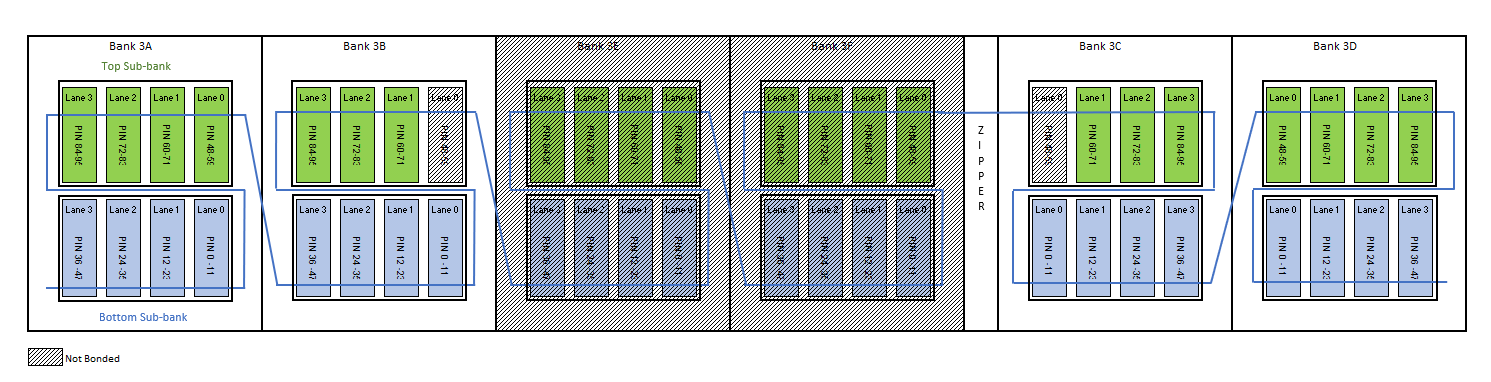
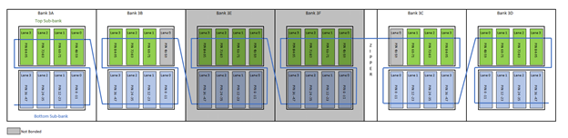
Figure 6. Sub-Bank Ordering in Top I/O Row in Intel® Agilex™ 7 F-Series and I-Series AGF012 and AGF014, package R24A/R24B
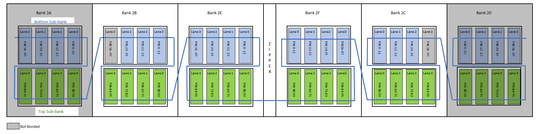
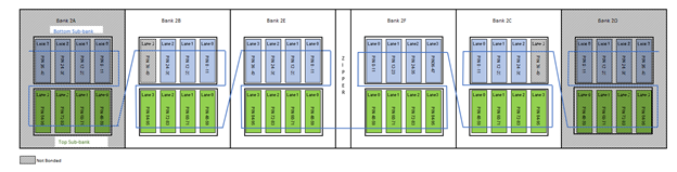
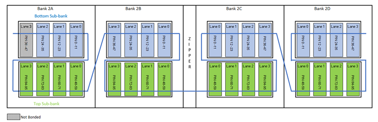
Figure 7. Sub-Bank Ordering in Bottom I/O Row in Intel® Agilex™ 7 F-Series and I-Series AGF012 and AGF014, package R24A/R24B
Figure 10. Sub-Bank Ordering in Top I/O Row in Intel® Agilex™ 7 F-Series and I-Series AGF022 and AGF027 devices, package R25A
On the top I/O row in AGF022 and AGF027 package R25A , an EMIF interface cannot span across Bank 3A and Bank 3F, because the two I/O banks are not adjacent to each other.
Figure 11. Sub-Bank Ordering in Bottom I/O Row in Intel® Agilex™ 7 F-Series and I-Series AGF022 and AGF027 devices, package R25A
Figure 12. Sub-Bank Ordering in Top I/O Row in Intel® Agilex™ 7 F-Series and I-Series AGI022 and AGI027 devices, package R29A
Bank 3E, Bank 3F, I/O Lane 0 in Top Sub-bank 3B and I/O Lane 0 in Top Sub-bank 3C are not bonded.
Figure 13. Sub-Bank Ordering in Bottom I/O Row in Intel® Agilex™ 7 F-Series and I-Series AGI022 and AGI027 devices, package R29A
Bank 2A, Bank 2D, I/O Lane 3 in Bottom Sub-bank 2B and I/O Lane 3 in Bottom Sub-bank 2C are not bonded.
Figure 14. Sub-Bank Ordering in Top I/O Row in Intel® Agilex™ 7 F-Series and I-Series AGI022 and AGI027 devices, package R31B

Bank 3E, Bank 3F, I/O Lane 0 in Top Sub-bank 3B and I/O Lane 0 in Top Sub-bank 3C are not bonded.
Figure 15. Sub-Bank Ordering in Bottom I/O Row in Intel® Agilex™ 7 F-Series and I-Series AGI022 and AGI027 devices, package R31B

Bank 2A, Bank 2B, I/O Lane 3 and I/O Lane 2 in Bottom Sub-bank 2E are not bonded.
Figure 16. Sub-Bank Ordering in Top I/O Row in Intel® Agilex™ 7 F-Series and I-Series AGF022 and AGF027 devices, package R31C
Bank 3E, Bank 3F, I/O Lane 0 in Top Sub-bank 3B and I/O Lane 0 in Top Sub-bank 3C are not bonded.
Figure 17. Sub-Bank Ordering in Bottom I/O Row in Intel® Agilex™ 7 F-Series and I-Series AGF022 and AGF027 devices, package R31C
Bank 2A, Bank 2B, I/O Lane 3 and I/O Lane 2 in Bottom Sub-bank 2E are not bonded
Figure 18. Sub-Bank Ordering in Top I/O Row in Intel® Agilex™ 7 F-Series and I-Series AGF022 and AGF027 devices, package R24C
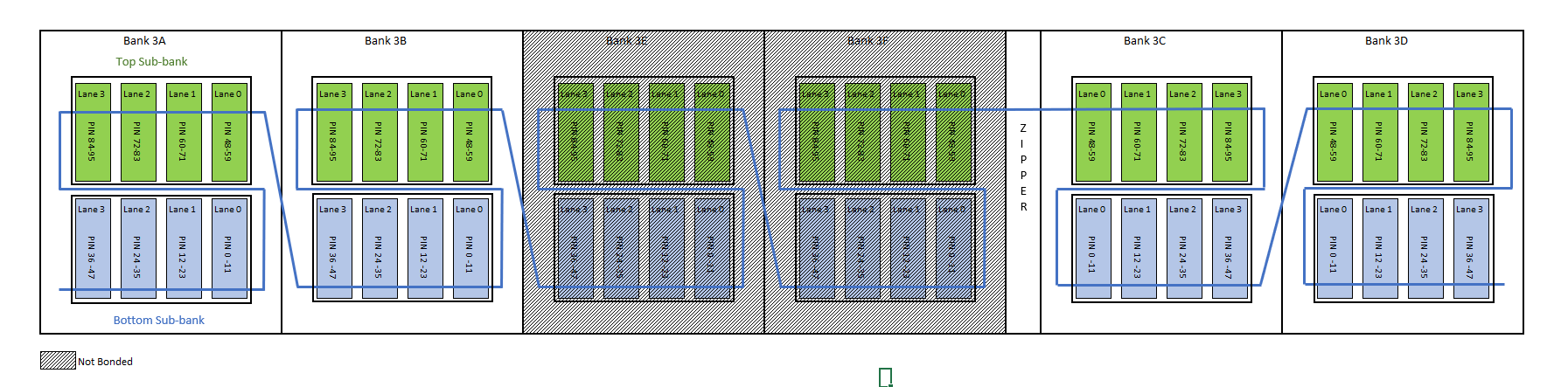
Figure 19. Sub-Bank Ordering in Bottom I/O Row in Intel® Agilex™ 7 F-Series and I-Series AGF022 and AGF027 devices, package R24C
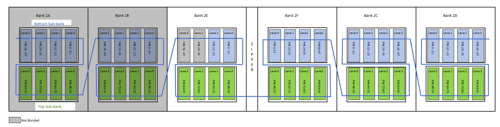
Figure 20. Sub-Bank Ordering in Top I/O Row in Intel® Agilex™ 7 F-Series and I-Series AGF019 and AGF023, package R25A
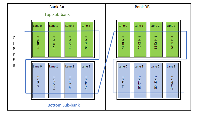
Figure 21. Sub-Bank Ordering in Bottom I/O Row in Intel® Agilex™ 7 F-Series and I-Series AGF019 and AGF023, package R25A
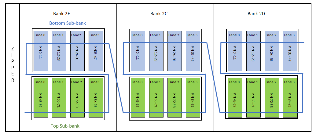
Figure 22. Sub-Bank Ordering in Top I/O Row in Intel® Agilex™ 7 F-Series and I-Series AGF006 and AGF008, package R16A
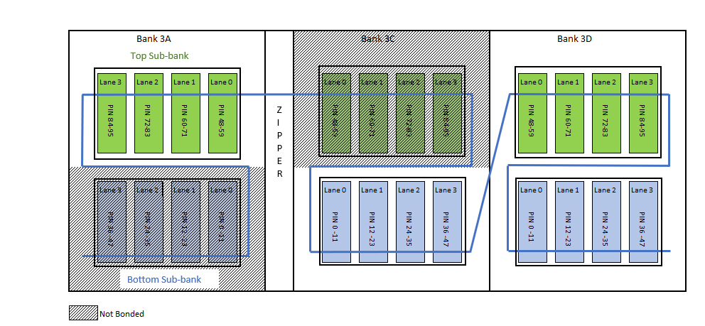
Figure 23. Sub-Bank Ordering in Bottom I/O Row in Intel® Agilex™ 7 F-Series and I-Series AGF006 and AGF008, package R16A
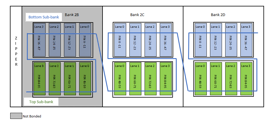
Figure 24. Sub-Bank Ordering in Top I/O Row in Intel® Agilex™ 7 F-Series and I-Series AGF006 and AGF008, package R24C
Figure 25. Sub-Bank Ordering in Bottom I/O Row in Intel® Agilex™ 7 F-Series and I-Series AGF006 and AGF008, package R24C
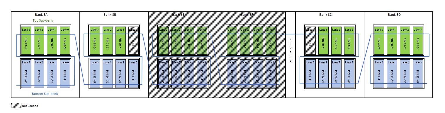
Figure 26. Sub-Bank Ordering in Top I/O Row in Intel® Agilex™ 7 F-Series and I-Series AGF012 and AGF014, package R24C
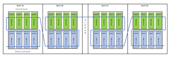
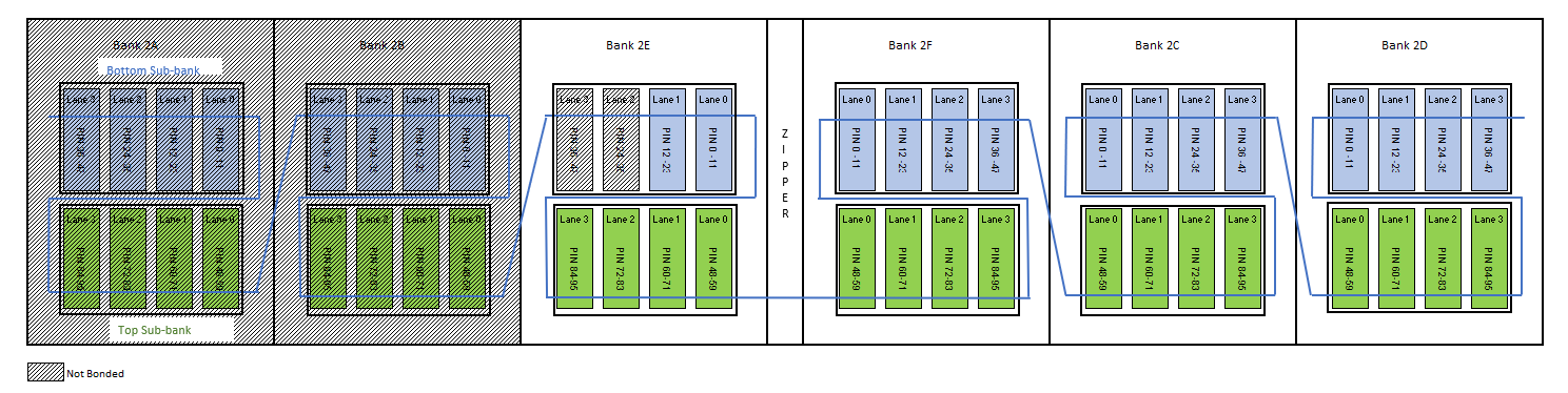
Figure 27. Sub-Bank Ordering in Bottom I/O Row in Intel® Agilex™ 7 F-Series and I-Series AGF012 and AGF014, package R24C
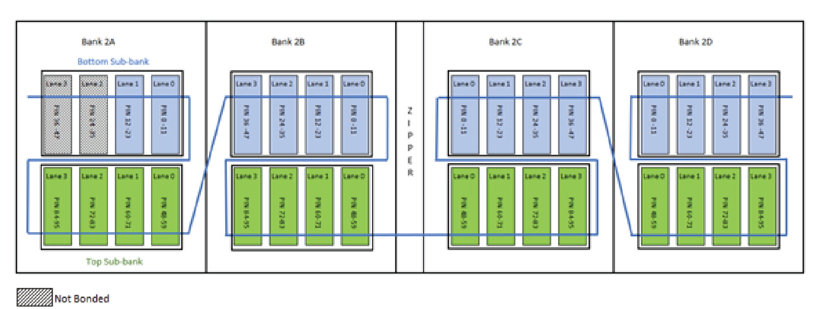
Figure 28. Sub-Bank Ordering in Top I/O Row in Intel® Agilex™ 7 F-Series and I-Series AGF019 and AGF023, package R24C

Figure 29. Sub-Bank Ordering in Bottom I/O Row in Intel® Agilex™ 7 F-Series and I-Series AGF019 and AGF023, package R24C

Figure 30. Sub-Bank Ordering in Top I/O Row in Intel® Agilex™ 7 F-Series and I-Series AGI019 and AGI023, package R31B
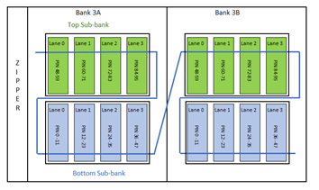
Figure 31. Sub-Bank Ordering in Bottom I/O Row in Intel® Agilex™ 7 F-Series and I-Series AGI019 and AGI023, package R31B

Figure 32. Sub-Bank Ordering in Top I/O Row in Intel® Agilex™ 7 F-Series and I-Series AGI019 and AGI023, package R18A

Figure 33. Sub-Bank Ordering in Bottom I/O Row in Intel® Agilex™ 7 F-Series and I-Series AGI019 and AGI023, package R18A
Figure 34. Sub-Bank Ordering in Top I/O Row in Intel® Agilex™ 7 F-Series and I-Series AGI035 and AGI040, package R39A
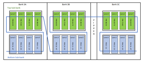
Figure 35. Sub-Bank Ordering in Bottom I/O Row in Intel® Agilex™ 7 F-Series and I-Series AGI035 and AGI040, package R39A
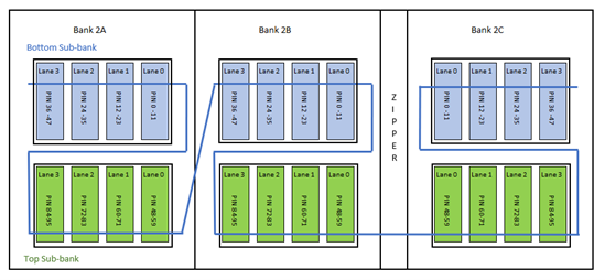
Figure 36. Sub-Bank Ordering in Top I/O Row in Intel® Agilex™ 7 F-Series and I-Series AGF019 and AGF023, package R31C
Figure 37. Sub-Bank Ordering in Bottom I/O Row in Intel® Agilex™ 7 F-Series and I-Series AGF019 and AGF023, package R31C
Figure 38. Sub-Bank Ordering in Top I/O Row in Intel® Agilex™ 7 F-Series and I-Series AGI027, package R29B
Bank 3E, Bank 3F, I/O Lane 0 in Top Sub-bank 3B and I/O Lane 0 in Top Sub-bank 3C are not bonded.
Figure 39. Sub-Bank Ordering in Bottom I/O Row in Intel® Agilex™ 7 F-Series and I-Series AGI027, package R29B
Bank 2A, Bank 2D, I/O Lane 3 in Bottom Sub-bank 2B and I/O Lane 3 in Bottom Sub-bank 2C are not bonded.
Figure 40. Sub-Bank Ordering in Top I/O Row in Intel® Agilex™ 7 F-Series and I-Series AGI041, package R29D
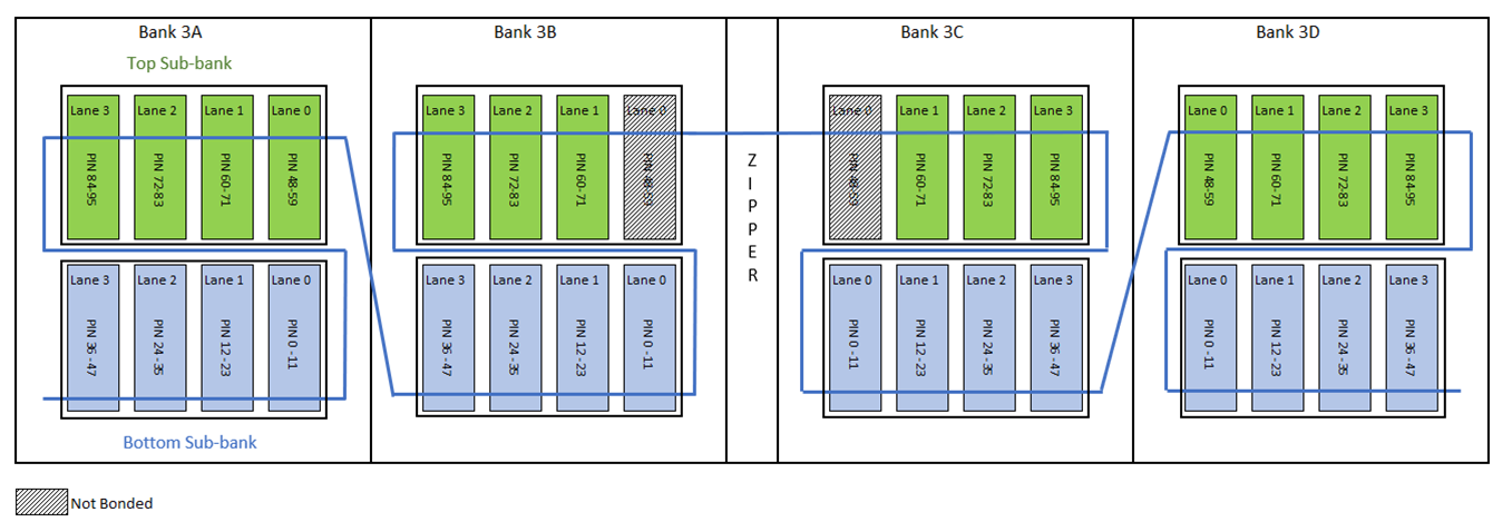
Figure 41. Sub-Bank Ordering in Bottom I/O Row in Intel® Agilex™ 7 F-Series and I-Series AGI041, package R29D
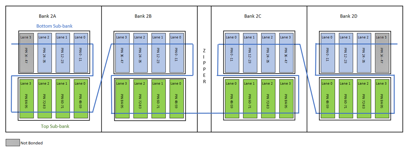
Figure 42. Sub-Bank Ordering in Top I/O Row in Intel® Agilex™ 7 F-Series and I-Series AGI022 and AGI027, package R31A
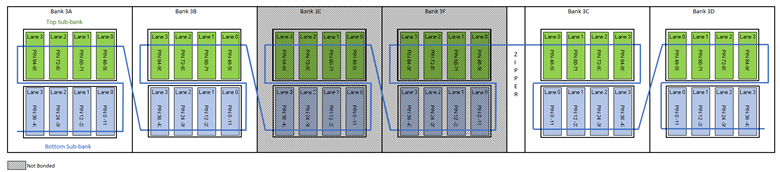
Figure 43. Sub-Bank Ordering in Bottom I/O Row in Intel® Agilex™ 7 F-Series and I-Series AGI022 and AGI027, package R31A
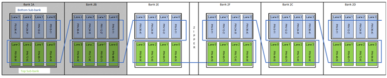
Figure 44. Sub-Bank Ordering in Top I/O Row in Intel® Agilex™ 7 F-Series and I-Series AGI041, package R31B
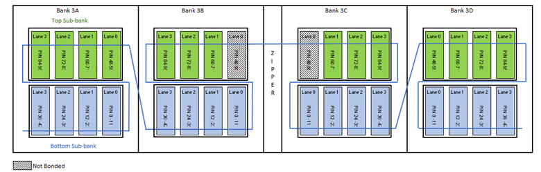
Figure 45. Sub-Bank Ordering in Bottom I/O Row in Intel® Agilex™ 7 F-Series and I-Series AGI041, package R31B
For AGI041 package R29D, pin JB26 and JH26 are available as REFCLK_GXRR15C_CH2p and REFCLK_GXRR15C_CH2n respectively on selected OPN. You must adhere to the layout guideline in “Restriction for using JB26, JH26, JP26 and JL27 on AGI041, Package R29D” section if you use the following pins:
- JB26 (REFCLK_GXRR15C_CH2p)
- JH26 (REFCLK_GXRR15C_CH2n)
- JP26 (I/O pin in Lane 2, Bottom Sub-bank of 2D)
- JL27 (I/O pin in Lane 2, Bottom Sub-bank of 2D)
The two sub-banks within an I/O bank are adjacent to each other when there is at least one I/O lane in each sub-bank that is bonded out and available for EMIF use. The blue line in the above figures shows the connectivity between the sub-banks.
For example, in the top row in Intel® Agilex™ 7 F-Series and I-Series AGF012 and AGF014 devices (Figure 6):
- The top sub-bank in 3A is adjacent to the bottom sub-bank in 3A and the bottom sub-bank in 3B.
- The top sub-bank in 3B is adjacent to the bottom sub-bank in 3B and the top sub-bank in 3C.
- The top sub-bank in 3B is adjacent to the top sub-bank in 3C even though there is a zipper block between the two sub-banks.
- The top sub-bank in 3B is not adjacent to the bottom sub-bank in 3A.
When an interface must occupy multiple sub-banks, ensure that those sub-banks are adjacent to one another. You can identify where a pin is located within an I/O bank based on its Index within I/O Bank value in the device pinout file.
Zipper Block
The zipper is a block that performs necessary routing adjustments where routing wires cross the zipper.
I/O Sub-Bank Usage
The pins in an I/O bank can serve as address and command pins, data pins, or clock and strobe pins for an external memory interface. You can implement a narrow interface, DDR4 x8 interface, with only a single I/O sub-bank. A wider interface of up to 72 bits can be implemented by configuring multiple adjacent sub-banks in a multi-bank interface.
Note: A given sub-bank cannot be shared between multiple EMIFs.
Note: For DDR4 hard PHY-only configurations, you can implement a minimum of x16 interface width up to a maximum of x72 interface width.
Every sub-bank includes a hard memory controller which you can configure for DDR4. In a multi-bank interface, only the controller of one sub-bank is active; controllers in the remaining sub-banks are turned off to conserve power.
To use a multi-bank Intel® Agilex™ 7 F-Series and I-Series EMIF interface, you must observe the following rules:
- Designate one sub-bank as the address and command bank.
- The address and command sub-bank must contain all the address and command pins.
- The locations of individual address and command pins within the address and command sub-bank must adhere to the pin map defined in the pin table— regardless of whether you use the hard memory controller or not. You can find the pin tables at the following location: https://www.intel.com/content/www/us/en/programmable/support/literature/lit-dp.html.
- If you do use the hard memory controller, the address and command sub-bank contains the active hard controller.
All the sub-banks are capable of functioning as the address and command bank. For interfaces that span multiple sub-banks, the Quartus® Prime software requires that the address and command bank be placed in the center-most bank of the interface. The only exception to this rule is for the Hardened Processor Subsystem External Memory Interface.