Visible to Intel only — GUID: zhw1500497748546
Ixiasoft
1. Overview
2. Implementing the Transceiver PHY Layer in L-Tile/H-Tile
3. PLLs and Clock Networks
4. Resetting Transceiver Channels
5. Intel® Stratix® 10 L-Tile/H-Tile Transceiver PHY Architecture
6. Reconfiguration Interface and Dynamic Reconfiguration
7. Calibration
8. Debugging Transceiver Links
A. Logical View of the L-Tile/H-Tile Transceiver Registers
2.1. Transceiver Design IP Blocks
2.2. Transceiver Design Flow
2.3. Configuring the Native PHY IP Core
2.4. Using the Intel® Stratix® 10 L-Tile/H-Tile Transceiver Native PHY Intel® Stratix® 10 FPGA IP Core
2.5. Implementing the PHY Layer for Transceiver Protocols
2.6. Unused or Idle Transceiver Channels
2.7. Simulating the Native PHY IP Core
2.8. Implementing the Transceiver Native PHY Layer in L-Tile/H-Tile Revision History
2.3.1. Protocol Presets
2.3.2. GXT Channels
2.3.3. General and Datapath Parameters
2.3.4. PMA Parameters
2.3.5. PCS-Core Interface Parameters
2.3.6. Analog PMA Settings Parameters
2.3.7. Enhanced PCS Parameters
2.3.8. Standard PCS Parameters
2.3.9. PCS Direct Datapath Parameters
2.3.10. Dynamic Reconfiguration Parameters
2.3.11. Generation Options Parameters
2.3.12. PMA, Calibration, and Reset Ports
2.3.13. PCS-Core Interface Ports
2.3.14. Enhanced PCS Ports
2.3.15. Standard PCS Ports
2.3.16. Transceiver PHY PCS-to-Core Interface Reference Port Mapping
2.3.17. IP Core File Locations
2.4.2.1. Receiver Word Alignment
2.4.2.2. Receiver Clock Compensation
2.4.2.3. Encoding/Decoding
2.4.2.4. Running Disparity Control and Check
2.4.2.5. FIFO Operation for the Enhanced PCS
2.4.2.6. Polarity Inversion
2.4.2.7. Data Bitslip
2.4.2.8. Bit Reversal
2.4.2.9. Byte Reversal
2.4.2.10. Double Rate Transfer Mode
2.4.2.11. Asynchronous Data Transfer
2.4.2.12. Low Latency
2.5.1.1. Transceiver Channel Datapath for PIPE
2.5.1.2. Supported PIPE Features
2.5.1.3. How to Connect TX PLLs for PIPE Gen1, Gen2, and Gen3 Modes
2.5.1.4. How to Implement PCI Express (PIPE) in Intel® Stratix® 10 Transceivers
2.5.1.5. Native PHY IP Core Parameter Settings for PIPE
2.5.1.6. fPLL IP Core Parameter Settings for PIPE
2.5.1.7. ATX PLL IP Core Parameter Settings for PIPE
2.5.1.8. Native PHY IP Core Ports for PIPE
2.5.1.9. fPLL Ports for PIPE
2.5.1.10. ATX PLL Ports for PIPE
2.5.1.11. Preset Mappings to TX De-emphasis
2.5.1.12. How to Place Channels for PIPE Configurations
2.5.1.13. Link Equalization for Gen3
2.5.1.14. Timing Closure Recommendations
3.1. PLLs
3.2. Input Reference Clock Sources
3.3. Transmitter Clock Network
3.4. Clock Generation Block
3.5. FPGA Fabric-Transceiver Interface Clocking
3.6. Double Rate Transfer Mode
3.7. Transmitter Data Path Interface Clocking
3.8. Receiver Data Path Interface Clocking
3.9. Channel Bonding
3.10. PLL Cascading Clock Network
3.11. Using PLLs and Clock Networks
3.12. PLLs and Clock Networks Revision History
4.1. When Is Reset Required?
4.2. Transceiver PHY Reset Controller Intel® Stratix® 10 FPGA IP Implementation
4.3. How Do I Reset?
4.4. Using PCS Reset Status Port
4.5. Using Transceiver PHY Reset Controller Intel® Stratix® 10 FPGA IP
4.6. Using a User-Coded Reset Controller
4.7. Combining Status or PLL Lock Signals with User Coded Reset Controller
4.8. Resetting Transceiver Channels Revision History
4.3.1.1. Resetting the Transmitter After Power Up
4.3.1.2. Resetting the Transmitter During Device Operation
4.3.1.3. Resetting the Receiver After Power Up
4.3.1.4. Resetting the Receiver During Device Operation (Auto Mode)
4.3.1.5. Clock Data Recovery in Manual Lock Mode
4.3.1.6. Special TX PCS Reset Release Sequence
4.5.1. Parameterizing Transceiver PHY Reset Controller Intel® Stratix® 10 FPGA IP
4.5.2. Transceiver PHY Reset Controller Intel® Stratix® 10 FPGA IP Parameters
4.5.3. Transceiver PHY Reset Controller Intel® Stratix® 10 FPGA IP Interfaces
4.5.4. Transceiver PHY Reset Controller Intel® Stratix® 10 FPGA IP Resource Utilization
5.1. PMA Architecture
5.2. Enhanced PCS Architecture
5.3. Intel® Stratix® 10 Standard PCS Architecture
5.4. Intel® Stratix® 10 PCI Express Gen3 PCS Architecture
5.5. PCS Support for GXT Channels
5.6. Square Wave Generator
5.7. PRBS Pattern Generator
5.8. PRBS Pattern Verifier
5.9. Loopback Modes
5.10. Intel® Stratix® 10 L-Tile/H-Tile Transceiver PHY Architecture Revision History
5.1.2.1.1. Programmable Differential On-Chip Termination (OCT)
5.1.2.1.2. Signal Detector
5.1.2.1.3. Continuous Time Linear Equalization (CTLE)
5.1.2.1.4. Variable Gain Amplifier (VGA)
5.1.2.1.5. Adaptive Parametric Tuning (ADAPT) Engine
5.1.2.1.6. Decision Feedback Equalization (DFE)
5.1.2.1.7. On-Die Instrumentation
5.2.1.1. TX Core FIFO
5.2.1.2. TX PCS FIFO
5.2.1.3. Interlaken Frame Generator
5.2.1.4. Interlaken CRC-32 Generator
5.2.1.5. 64B/66B Encoder and Transmitter State Machine (TX SM)
5.2.1.6. Scrambler
5.2.1.7. Interlaken Disparity Generator
5.2.1.8. TX Gearbox, TX Bitslip and Polarity Inversion
5.2.1.9. KR FEC Blocks
5.2.2.1. RX Gearbox, RX Bitslip, and Polarity Inversion
5.2.2.2. Block Synchronizer
5.2.2.3. Interlaken Disparity Checker
5.2.2.4. Descrambler
5.2.2.5. Interlaken Frame Synchronizer
5.2.2.6. 64B/66B Decoder and Receiver State Machine (RX SM)
5.2.2.7. 10GBASE-R Bit-Error Rate (BER) Checker
5.2.2.8. Interlaken CRC-32 Checker
5.2.2.9. RX PCS FIFO
5.2.2.10. RX Core FIFO
5.3.1.4.1. 8B/10B Encoder Control Code Encoding
5.3.1.4.2. 8B/10B Encoder Reset Condition
5.3.1.4.3. 8B/10B Encoder Idle Character Replacement Feature
5.3.1.4.4. 8B/10B Encoder Current Running Disparity Control Feature
5.3.1.4.5. 8B/10B Encoder Bit Reversal Feature
5.3.1.4.6. 8B/10B Encoder Byte Reversal Feature
5.3.2.1.1. Word Aligner Bitslip Mode
5.3.2.1.2. Word Aligner Manual Mode
5.3.2.1.3. Word Aligner Synchronous State Machine Mode
5.3.2.1.4. Word Aligner Deterministic Latency Mode
5.3.2.1.5. Word Aligner Pattern Length for Various Word Aligner Modes
5.3.2.1.6. Word Aligner RX Bit Reversal Feature
5.3.2.1.7. Word Aligner RX Byte Reversal Feature
5.3.2.6.1. Byte Deserializer Disabled Mode
5.3.2.6.2. Byte Deserializer Deserialize x2 Mode
5.3.2.6.3. Byte Deserializer Deserialize x4 Mode
5.3.2.6.4. Bonded Byte Deserializer
5.3.2.6.5. Byte Ordering Register-Transfer Level (RTL)
5.3.2.6.6. Byte Serializer Effects on Data Propagation at the RX Side
5.3.2.6.7. ModelSim Byte Ordering Analysis
6.1. Reconfiguring Channel and PLL Blocks
6.2. Interacting with the Reconfiguration Interface
6.3. Multiple Reconfiguration Profiles
6.4. Arbitration
6.5. Recommendations for Dynamic Reconfiguration
6.6. Steps to Perform Dynamic Reconfiguration
6.7. Direct Reconfiguration Flow
6.8. Native PHY IP or PLL IP Core Guided Reconfiguration Flow
6.9. Reconfiguration Flow for Special Cases
6.10. Changing Analog PMA Settings
6.11. Ports and Parameters
6.12. Dynamic Reconfiguration Interface Merging Across Multiple IP Blocks
6.13. Embedded Debug Features
6.14. Timing Closure Recommendations
6.15. Unsupported Features
6.16. Transceiver Register Map
6.17. Reconfiguration Interface and Dynamic Revision History
7.5.1. Recalibrating a Duplex Channel (Both PMA TX and PMA RX)
7.5.2. Recalibrating the PMA RX Only in a Duplex Channel
7.5.3. Recalibrating the PMA TX Only in a Duplex Channel
7.5.4. Recalibrating a PMA Simplex RX Without a Simplex TX Merged into the Same Physical Channel
7.5.5. Recalibrating a PMA Simplex TX Without a Simplex RX Merged into the Same Physical Channel
7.5.6. Recalibrating Only a PMA Simplex RX in a Simplex TX Merged Physical Channel
7.5.7. Recalibrating Only a PMA Simplex TX in a Simplex RX Merged Physical Channel
7.5.8. Recalibrating the fPLL
7.5.9. Recalibrating the ATX PLL
7.5.10. Recalibrating the CMU PLL When it is Used as a TX PLL
A.4.1. Transmitter PMA Logical Register Map
A.4.2. Receiver PMA Logical Register Map
A.4.3. Pattern Generators and Checkers
A.4.4. Loopback
A.4.5. Optional Reconfiguration Logic PHY- Capability
A.4.6. Optional Reconfiguration Logic PHY- Control & Status
A.4.7. Embedded Streamer (Native PHY)
A.4.8. Static Polarity Inversion
A.4.9. Reset
A.4.10. CDR/CMU and PMA Calibration
Visible to Intel only — GUID: zhw1500497748546
Ixiasoft
2.4.3.1.2. FIFO Latency Calculation
Latency through FIFOs (in PC mode) may vary from reset to reset. You can determine that variation by using the appropriate FIFO latency calculation logic. The phase measuring technique measures the distance between read and write counters. The phase measuring circuit is designed to work in the case of a phase comp FIFO and in the case of a phase comp FIFO where the read and write pointers may have an exact 2:1 ratio.
To measure the fullness of the FIFO, run your sampling clock at a rate that is not equal to the parallel clock. The guideline for calculating the sampling clock is that the sampling clock sweeps various phase relationships relative to the parallel clock. Using a simple counter, you should determine how often the resulting pulse is a 1 versus a 0. You can find this implementation in the FIFO latency calculation logic referenced below.
Figure 85. Phase Measuring FIFO
Below is an example implementation of the FIFO latency calculation logic. Each FIFO in phase compensation mode has a latency measurement port (read only) available at the PCS-Core interface. Each latency measurement port supplies the latency pulse whose duty cycle depends on the FIFO latency. This latency pulse is further processed in the FPGA fabric to calculate FIFO latency. There are four similar pulses for the four FIFOs, and you must perform latency calculations on all of them separately. The IP represented in the following figure represents the logic in the FPGA fabric that performs the latency calculation. This IP is not a part of the Native PHY IP core, so you must instantiate it exclusively. Output of the IP is the Total FIFO count bus. This bus produces the result of the FIFO latency calculation. This result can only be read when the calculation is complete, and is denoted by the result_ready signal coming out of the IP. Refer to FIFO Latency Calculation.
Figure 86. FIFO Latency Calculation
Once result_ready is asserted, you can read data on the Total FIFO count bus and calculate latency time using the following equation.
Figure 87. FIFO Latency Formula
The latency pulse available at a latency measurement port of a FIFO appears as shown below. The duty cycle of the pulse depends on the difference between the read and write pointers at a particular instant. The duty cycle of a pulse varies with time as both read and write pointers move. To find the actual latency through the FIFO, the IP block calculates the average of latency pulse duty cycles for an appropriate duration.
As seen in the figure below, a sampling clock (LATENCY_SCLK) samples the pulse. After the sampling duration, all the samples of 1s are accumulated and appear at the Total FIFO count output bus, which is then used in FIFO Latency Calculation to calculate latency (in nsec). The Number of pulses parameter is the actual number of latency pulses for which the latency calculation logic executes. This parameter defines the execution time of the latency calculation logic. The design file referenced below defaults to 128 latency pulses to calculate FIFO latency. Due to hardware limitations, the sampling clock cannot be higher than 260 MHz.
Figure 88. FIFO Latency Measurement Port Number of pulses and the LATENCY_SCLK period vary depending on your particular implementation.
Figure 89. FIFO Latency Calculation Logic
| Symbol | Input/Output | Description |
|---|---|---|
| latency_sclk | Input | Sampling clock required by the latency calculation logic |
| start_calc | Input | Control signal to start the latency calculation |
| fifo_latency_pulse | Input | Latency pulse |
| total_fifo_count | Output | Result from the latency calculation logic |
| result_ready | Output | Status signal that signifies completion of the latency calculation logic |
Figure 90. FIFO Latency Calculation Logic for Four FIFOsPoint A is the assertion of start_calc signals, and point B is an assertion of result_ready signals. The total_fifo_count signal is valid after result_ready is asserted.
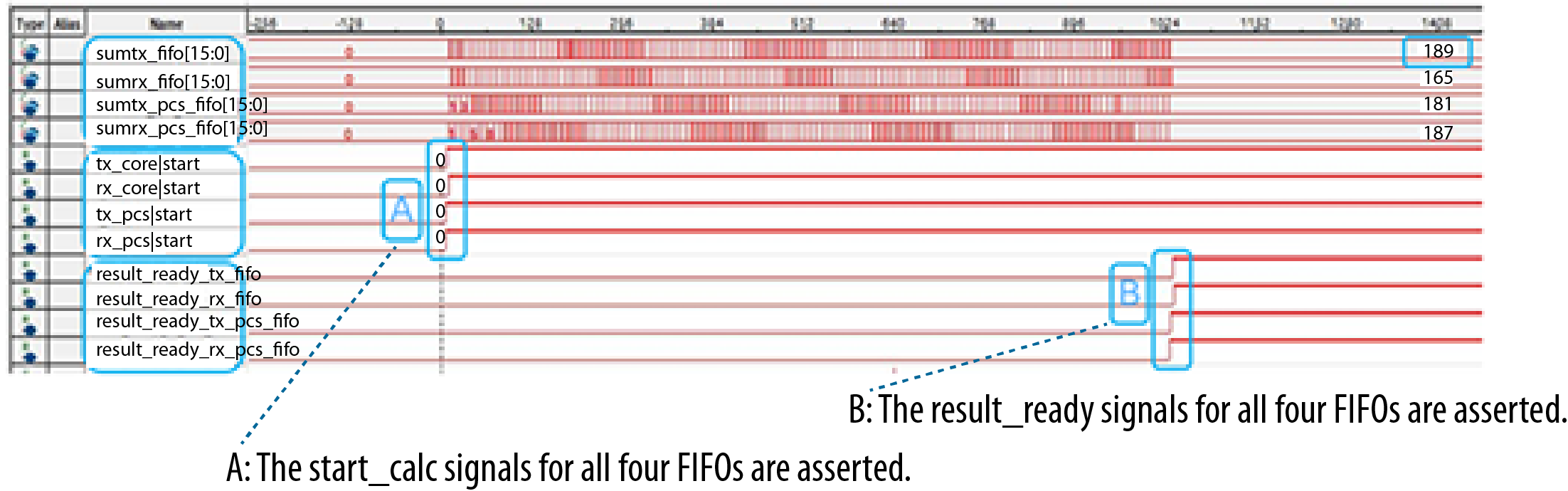
Figure 91. FIFO Latency Formula for all FIFOs
Follow these guidelines for the preferred frequency for latency_sclk:
- latency_sclk must be ≤ 260 MHz.
- The ratio of parallel clock to latency_sclk, when expressed in lowest terms, should have denominator of at least 50, but preferably, more than 100. The ideal resultant latency_sclk should be between 200 MHz to 260 MHz.
- Do not use a latency_sclk frequency that is a multiple of tx_clkout.
- Examples:
Table 92. Parallel Clock to latency_sclk Ratio Scenarios tx_clkout Frequency Correct latency_sclk Frequency Incorrect latency_sclk Frequency 150 MHz 209 MHz 160 MHz 245 MHz 247 MHz 250 MHz 300 MHz 247 MHz 260 MHz
You can create latency_sclk using the IOPLL or the external reference clock.
Related Information