Visible to Intel only — GUID: rnw1528176155818
Ixiasoft
2.1.1. Directory Structure
2.1.2. Generating the Design
2.1.3. Simulating the E-tile Ethernet IP for Intel Agilex FPGA Design Example Testbench
2.1.4. Compiling the Compilation-Only Project
2.1.5. Compiling and Configuring the Design Example in Hardware
2.1.6. Testing the E-tile Ethernet IP for Intel Agilex FPGA Hardware Design Example
2.2.1.1. Non-PTP 10GE/25GE MAC+PCS with Optional RS-FEC Simulation Design Example
2.2.1.2. PTP 10GE/25GE MAC+PCS with Optional RS-FEC Simulation Design Example
2.2.1.3. 10GE/25GE PCS Only, OTN, or FlexE with Optional RS-FEC Simulation Design Example
2.2.1.4. 10GE/25GE Custom PCS with Optional RS-FEC Simulation Design Example
2.3.1. Simulation Design Examples
2.3.2. Hardware Design Examples
2.3.3. 100GE MAC+PCS with Optional RS-FEC Design Example Interface Signals
2.3.4. 100GE PCS with Optional RS-FEC Design Example Interface Signals
2.3.5. 100GE MAC+PCS with Optional RS-FEC Design Example Registers
2.3.6. 100GE PCS with Optional RS-FEC Design Example Registers
2.3.1.1. Non-PTP E-tile Ethernet IP for Intel Agilex FPGA 100GE MAC+PCS with Optional RS-FEC Simulation Design Example
2.3.1.2. E-tile Ethernet IP for Intel Agilex FPGA 100GE MAC+PCS with Optional RS-FEC and PTP Simulation Design Example
2.3.1.3. E-tile Ethernet IP for Intel Agilex FPGA 100GE PCS Only with Optional RS-FEC Simulation Design Example
2.3.1.4. E-tile Ethernet IP for Intel Agilex FPGA 100GE OTN with Optional RS-FEC Simulation Design Example
2.3.1.5. E-tile Ethernet IP for Intel Agilex FPGA 100GE FlexE with Optional RS-FEC Simulation Design Example
3.1.1. Hardware and Software Requirements
3.1.2. Generating the Design
3.1.3. Directory Structure
3.1.4. Simulating the Design Example Testbench
3.1.5. Compiling the Compilation-Only Project
3.1.6. Compiling and Configuring the Design Example in Hardware
3.1.7. Testing the E-tile CPRI PHY Intel® FPGA IP Hardware Design Example
4.1. Quick Start Guide
4.2. 10G/25G Ethernet Dynamic Reconfiguration Design Examples
4.3. 25G Ethernet to CPRI Dynamic Reconfiguration Design Example
4.4. CPRI Dynamic Reconfiguration Design Examples
4.5. 100G Ethernet Dynamic Reconfiguration Design Example
4.6. Document Revision History for the E-tile Dynamic Reconfiguration Design Example
4.5.1. Functional Description
4.5.2. Testing the 100G Ethernet Dynamic Reconfiguration Hardware Design Example
4.5.3. Simulation Design Examples
4.5.4. 100GE DR Hardware Design Examples
4.5.5. 100G Ethernet Dynamic Reconfiguration Design Example Interface Signals
4.5.6. 100G Ethernet Dynamic Reconfiguration Examples Registers
4.5.7. Steps to Enable FEC
4.5.8. Steps to Disable FEC
Visible to Intel only — GUID: rnw1528176155818
Ixiasoft
2.1.2. Generating the Design
Procedure
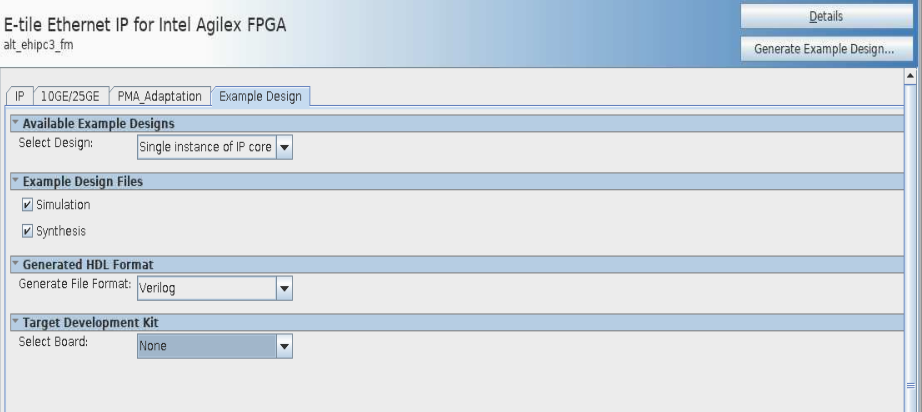
Example Design Tab in the E-tile Ethernet IP for Intel Agilex FPGA Parameter Editor
Follow these steps to generate the E-tile Ethernet IP for Intel Agilex FPGA testbench:
- In the IP Catalog, locate and select E-tile Ethernet IP for Intel Agilex FPGA . The New IP Variation window appears.
- Specify a top-level name <your_ip> for your custom IP variation. The parameter editor saves the IP variation settings in a file named <your_ip> .ip.
- Click OK. The parameter editor appears.
- On the IP, 100GE, or 10GE/25GE tabs, specify the parameters for your IP core variation.
- Change PMA adaptation setting. To change the PMA adaptation setting for the optimal performance, go to PMA Adaptation tab. This step is optional.
- Select a PMA adaptation preset for PMA adaptation Select parameter.
- Click PMA Adaptation Preload to load the initial and continuous adaptation parameters.
- Specify the number of PMA configurations to support when multiple PMA configurations are enabled using Number of PMA configuration parameter.
- Select which PMA configuration to load or store using Select a PMA configuration to load or store.
- Click Load adaptation from selected PMA configuration to load the selected PMA configuration settings.
For more information about the PMA adaptation parameters, refer to the E-Tile Transceiver PHY User Guide.
Note: If you require more information about the PMA adaptation parameters, contact My Intel support. - On the Example Design tab, under Example Design Files, select the Simulation option to generate the testbench and the compilation-only project. Select the Synthesis option to generate the hardware design example. You must select at least one of the Simulation and Synthesis options to generate the design example.
- On the Example Design tab, under Generated HDL Format, select Verilog HDL or VHDL. If you select VHDL, you must simulate the testbench with a mixed-language simulator. The device under test in the ex_<datarate> directory is a VHDL model, but the main testbench file is a System Verilog file.
- Under Target Development Kit, select the Agilex F-series Transceiver-SoC Development Kit - AGFB014R24A2E2V, Agilex F-series Transceiver-SoC Development Kit - AGFB014R24A2E2VR0 or select None. If you select a specific Development Kit as the Target Development Kit, the design example is generated based on a specific device and it overwrites the device you selected in your project file. If you select None as the Target Development Kit, ensure the selected device is your targeted device and adjust the pins assignment in the .qsf file. By default, .qsf file is generated based on the device used in the development kit
- Click the Generate Example Design button. The Select Example Design Directory window appears.
- If you want to modify the design example directory path or name from the defaults displayed (alt_ehipc3_ fm_ 0_example_design), browse to the new path and type the new design example directory name (<design_example_dir>).