Visible to Intel only — GUID: ieu1485902661246
Ixiasoft
1.7.1. Stratix® 10 Device Recommendations
1.7.2. Stratix® V Device Recommendations
1.7.3. Stratix IV Device Recommendations
1.7.4. Arria® 10 Device Recommendations
1.7.5. Arria® V Device Recommendations
1.7.6. Arria II Device Recommendations
1.7.7. Cyclone® 10 Device Recommendations
1.7.8. Cyclone® V Device Recommendations
1.7.9. Cyclone® IV Device Recommendations
1.7.10. Cyclone III Device Recommendations
Visible to Intel only — GUID: ieu1485902661246
Ixiasoft
1.4.2. Signal Layers
In high-density FPGAs, many signal layers are required to achieve full breakout of all available I/Os.
A good estimate for the minimum number of signal layers required is to count the depth of the row or column I/O signal balls of the FPGA device, divide that number by two, and round up to the nearest even whole number.
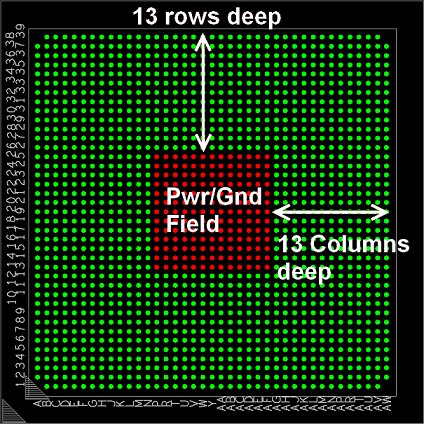
For example, on a Stratix IV GX device in an F1517 BGA package, the I/O row and column span 13 deep as shown in below figure. Therefore, a minimum of seven signal layers are required for a complete I/O signal breakout for that device. However, for a balanced PCB stackup, eight signals layers must be used.
Figure 4. BGA I/O Signal Depth
After the dedicated signal layers are determined, they must be arranged within the stackup. To maintain impedance control and provide a current return path, signal layers require an accompanying reference plane layer. Depending on whether microstrip or stripline topologies are used, several stackup construction choices are available.
Below figure (left) shows a microstrip construction. The Signal-Plane topology (S-P) places the signal layer on the surface of the PCB (either top or bottom) with a reference plane layer directly adjacent to the signal layer. With this topology, the difference between εr of air on one side and εr of the dielectric material on the other side causes odd and even mode trace velocity differences that result in far-end crosstalk in differential pair routing. One way to mitigate this situation when using microstrip routing is to use an embedded microstrip, where a thin layer of epoxy or soldermask is added over the surface traces to make εr more uniform, as shown in below figure (right).
Figure 5. Microstrip Signal Topologies
In a stripline construction, the single stripline topology uses Plane-Signal-Plane (P-S-P) to provide the best signal isolation but requires more layers for complete signal isolation. As a result, a more commonly used stripline construction is the dual stripline. This Plane-Signal-Signal-Plane (P-S-S-P) topology results in more efficient layer usage, but care must be observed to manage adjacent layer coupling. This coupling is usually reduced in the stackup design by increasing the adjacent signal-to-signal separation compared to the signal-to-plane separation. Doing this forces the majority of the return current along the reference plane layer directly above or below the signal instead of onto the adjacent signal layer. However, having large separations adds to the overall thickness of the board. This can impact standard board manufacturing if the aspect ratio of the via drill to board thickness is larger than 10:1. In addition to layer separation, signal-to-signal coupling can also be minimized by routing adjacent layers orthogonally to each other to minimize the overlapping coupling region. An added benefit of stripline routing is zero far-end crosstalk because of a uniform εr surrounding the signal traces.
Figure 6. Stripline Signal Topologies