Visible to Intel only — GUID: joc1463362604091
Ixiasoft
Intel® Stratix® 10 Devices and Transceiver Channels
PCB Stackup Selection Guideline
Recommendations for High Speed Signal PCB Routing
FPGA Fan-out Region Design
CFP2/CFP4 Connector Board Layout Design Guideline
QSFP+/zSFP/QSFP28 Connector Board Layout Design Guideline
SMA 2.4-mm Layout Design Guideline
Tyco/Amphenol Interlaken Connector Design Guideline
Electrical Specifications
Document Revision History for AN 766: Intel® Stratix® 10 Devices, High Speed Signal Interface Layout Design Guideline
Option 1: Via-In-Pad Topology
Option 2: Dog-bone with GND Cutout at BGA Pad Topology
Option 3: Micro-via Topology
GND Cutout Under BGA Pads in Fan-out Configuration
Comparison of Dog-bone with GND Cutout Under the BGA and Via-in-Pad Configurations
Trace Shape Routing at the BGA Void Area (Tear Drop Configuration)
Visible to Intel only — GUID: joc1463362604091
Ixiasoft
QSFP+ Module Assembly and Pinout
The Quad Small Form-factor Pluggable (QSFP) specification is based on the SFF-8665, SFF-8679 and OIF CEI v3.1 standards.
Figure 75. Simplified QSFP+ Channel
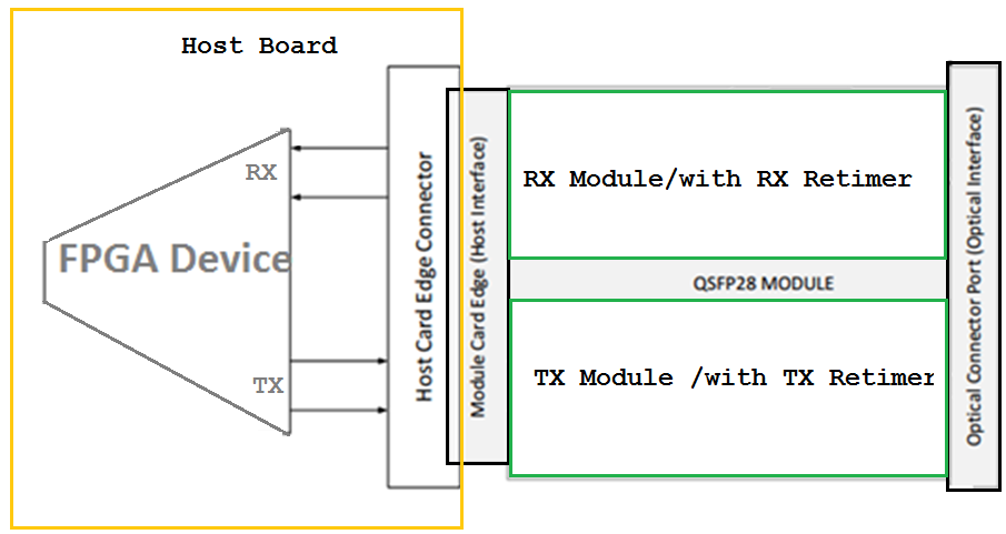
The roadmap for QSFP+ standards operating up to 28 Gbps includes:
- 10 Gbps QSFP10 SFF-8635
- 14 Gbps QSFP14 SFF-8685
- 28 Gbps QSFP28 SFF-8665
Figure 76. QSFP+ Module and Pin Map Layout
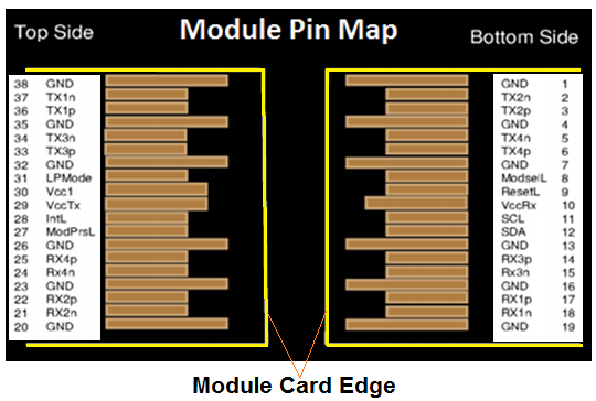
The RX(n)(p/n) and TX(n)(p/n) are module receiver data outputs and transmitter data inputs. They are all AC-coupled 100 Ω differential lines that should be terminated with 100 Ω differentially at the Host ASIC (SerDes). The AC coupling is inside the module and not required on the host board. For operation at 28 Gbps the relevant standards (OIF-CEI-03.1 standard document) define the signal requirements on the high-speed differential lines. For operation at lower rates, refer to the appropriate standards.