Visible to Intel only — GUID: vgo1449736080450
Ixiasoft
1.4.1. Use Case 1: Source Synchronous I/O Interface
1.4.2. Use Case 2: Driving Data from FPGA through GPIO to External Device
1.4.3. Use Case 3: Multiple-Speed Parallel Interfaces
1.4.4. Use Case 4: GPIO Interface Using 3.0V/2.5V I/O Standard
1.4.5. Use Case 5: Generating Output Clock through GPIO Output Pin
Visible to Intel only — GUID: vgo1449736080450
Ixiasoft
1.5.2. Design Verification
You can verify the Altera GPIO to Altera PHYLite design example using the Intel® Arria® 10 FPGA development kit.
To verify the design example, you require the following hardware:
- Arria® 10 FPGA development kit
- Loopback FPGA Mezzanine Card (FMC) attached to the FMC port B (FMCB)
- Intel® FPGA Download Cable II
The design example demonstrates a simple loopback that loops back the fixed serial 1100 pattern transmitted from the Altera PHYLite output (ddr_out) to the Altera PHYLite input (ddr_in) through the Loopback FMC daughter card.
The Altera PHYLite output signals from the dataout and clkout pins connect directly to the data_in and strobe_in pins that feed the Altera PHYLite input.
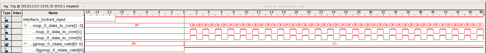
The data received from the Altera PHYLite input after you program the SOF in the Signal Tap Logic Analyzer should be the same as the data transmitted from the IP core through the Altera PHYLite output.
Figure 17. Signal Tap Results for Data from the IP CoreThis figure shows the Signal Tap results captured for the data from the IP core, (using the auto_signaltap_0 instance in the .stp file).

Figure 18. Signal Tap Results for Data to the IP CoreThis figure shows the Signal Tap results captured for the data to the IP core after the rdata_valid signal goes high, (using the auto_signaltap_1 instance in the .stp file).