Visible to Intel only — GUID: ewa1437423807285
Ixiasoft
1. Intel® FPGA SDK for OpenCL™ Intel® Arria® 10 GX FPGA Development Kit Reference Platform Porting Guide
2. Developing Your Intel® Arria® 10 Custom Platform
3. Intel® Arria® 10 GX FPGA Development Kit Reference Platform Design Architecture
4. Intel® FPGA SDK for OpenCL™ Intel® Arria® 10 GX FPGA Development Kit Reference Platform Porting Guide Archives
5. Document Revision History for the Intel Arria 10 GX FPGA Development Kit Reference Platform Porting Guide
1.1. Intel® Arria® 10 GX FPGA Development Kit Reference Platform: Prerequisites
1.2. Features of the Intel® Arria® 10 GX FPGA Development Kit Reference Platform
1.3. Contents of the Intel® Arria® 10 GX FPGA Development Kit Reference Platform
1.4. Intel Arria 10 GX FPGA Development Kit Reference Platform BSP Changes Between Intel® Quartus® Prime Design Suite Releases
1.4.1. BSP Changes from Intel® Quartus® Prime Design Suite Version 16.1 to Version 17.0
1.4.2. BSP Changes from Intel® Quartus® Prime Design Suite Version 17.0 to Version 17.1
1.4.3. BSP Changes from Intel® Quartus® Prime Design Suite Version 17.1 to Version 18.0
1.4.4. BSP Changes from Intel® Quartus® Prime Design Suite Version 18.0 to Version 18.1
1.4.5. BSP Changes from Intel® Quartus® Prime Design Suite Version 18.1 to Version 19.1
2.1. Initializing Your Intel® Arria® 10 Custom Platform
2.2. Modifying the Intel® Arria® 10 GX FPGA Development Kit Reference Platform Design
2.3. Integrating Your Intel® Arria® 10 Custom Platform with the Intel® FPGA SDK for OpenCL™
2.4. Setting up the Intel® Arria® 10 Custom Platform Software Development Environment
2.5. Establishing Intel® Arria® 10 Custom Platform Host Communication
2.6. Branding Your Intel® Arria® 10 Custom Platform
2.7. Changing the Device Part Number
2.8. Connecting the Memory in the Intel® Arria® 10 Custom Platform
2.9. Modifying the Kernel PLL Reference Clock
2.10. Integrating an OpenCL Kernel in Your Intel® Arria® 10 Custom Platform
2.11. Guaranteeing Timing Closure in the Intel® Arria® 10 Custom Platform
2.12. Troubleshooting Intel® Arria® 10 GX FPGA Development Kit Reference Platform Porting Issues
3.1. Host-to- Intel® Arria® 10 FPGA Communication over PCIe®
3.2. DDR4 as Global Memory for OpenCL Applications
3.3. Host Connection to OpenCL Kernels
3.4. Intel® Arria® 10 FPGA System Design
3.5. Dynamic PLL Reconfiguration
3.6. Guaranteed Timing Closure of the Intel® Arria® 10 GX FPGA Development Kit Reference Platform Design
3.7. Intel® Quartus® Prime Compilation Flow and Scripts
3.8. Addition of Timing Constraints
3.9. Connection of the Intel® Arria® 10 GX FPGA Development Kit Reference Platform to the Intel® FPGA SDK for OpenCL™
3.10. Intel® Arria® 10 FPGA Programming Flow
3.11. Host-to-Device MMD Software Implementation
3.12. Implementation of Intel® FPGA SDK for OpenCL™ Utilities
3.13. Intel® Arria® 10 FPGA Development Kit Reference Platform Scripts
3.14. Considerations in Intel® Arria® 10 GX FPGA Development Kit Reference Platform Implementation
3.1.1. Instantiation of Intel® Arria® 10 PCIe* Hard IP with Direct Memory Access
3.1.2. Device Identification Registers for Intel® Arria® 10 PCIe Hard IP
3.1.3. Instantiation of the version_id Component
3.1.4. Definitions of Intel® Arria® 10 FPGA Development Kit Reference Platform Hardware Constraints in Software Headers Files
3.1.5. PCIe Kernel Driver for the Intel® Arria® 10 GX FPGA Development Kit Reference Platform
3.1.6. Direct Memory Access
3.1.7. Message Signaled Interrupt
3.1.8. Partial Reconfiguration
3.1.9. Cable Autodetect
3.1.10. Host Channel
Visible to Intel only — GUID: ewa1437423807285
Ixiasoft
3.4.3. Floorplan
Intel® establishes the floorplan of the Intel® Arria® 10 GX FPGA Development Kit Reference Platform by iterating on the design and IP placements.
Dependencies
- Partial Reconfiguration
- Chip Planner
- Logic Lock Plus regions
Intel® performed the following tasks iteratively to derive the floorplan of the a10_ref Reference Platform:
- Compile a design without any region or floorplanning constraints.
Intel® recommends that you compile the design with several seeds.
- Examine the placement of the IP cores (for example, PCIe* , DDR4, Avalon® interconnect pipeline stages and adapters) for candidate locations, as determined by the Intel® Quartus® Prime Pro Edition software's Fitter. In particular, Intel® recommends examining the seeds that meet or almost meet the timing constraints.
For the a10_ref Reference Platform, the PCIe* I/O is located in the lower left corner of the Intel® Arria® 10 FPGA. The DDR4 I/O is located on the top part of the left I/O column of the device. Because the placements of the PCIe and DDR4 IP components tend to be close to the locations of their respective I/Os, you can apply Logic Lock Plus regions to constrain the IP components to those candidate regions.
Figure 2. Floorplan of the Intel® Arria® 10 FPGA Development Kit Reference Platform
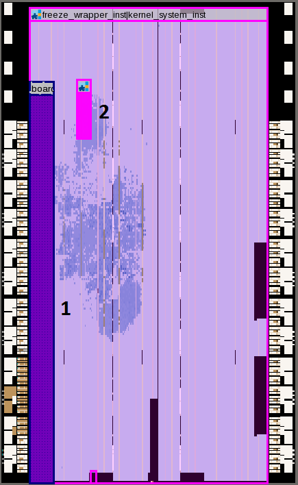
As shown in this Chip Planner view of the floorplan, the two Logic Lock Plus regions are spread out between the PCIe I/O and the top region of the left I/O column (that is, the DDR4 I/O area).
- The largest Logic Lock Plus region (Region 1) covers the PCIe I/O and contains most of the static board interface logic.
- Regions 2 contains an Avalon interconnect pipeline stage that bridges the PCIe I/O and DDR4 I/O regions. The Avalon interconnect pipeline stages also help improve the timing closure rate of the static board interface part of the design.
You must create a dedicated Logic Lock Plus region for the OpenCL™ kernel system. Furthermore, do not place kernel logic in the board's Logic Lock Plus regions (that is, static region). The static region and the OpenCL kernel system region (that is, PR region) do not overlap each other. As shown in Floorplan of the Intel® Arria® 10 FPGA Development Kit Reference Platform, the logic for the boardtest.cl OpenCL kernel, that is, the scatter area, can be placed anywhere except within the seven Logic Lock Plus regions.
Intel® recommends the following strategies to maximize the available FPGA resources for the OpenCL kernel system to improve kernel routability:
- The OpenCL kernel system PR region should cover the entire device except the Logic Lock Plus regions of the board.
- The size of a Logic Lock Plus region should be just large enough to contain the board logic and to meet timing constraints of the board clocks. Oversized Logic Lock Plus regions consume FPGA resources unnecessarily.
- Avoid creating tightly-packed Logic Lock Plus regions that cause very high logic utilization and high routing congestion.
High routing congestion within the Logic Lock Plus regions might decrease the Fitter's ability to route OpenCL kernel signals through the regions.
In the case where the board clocks are not meeting timing and the critical path is between the Logic Lock Plus regions (that is, across region-to-region gap), insert back-to-back pipeline stages on paths that cross the gap. For example, if the critical path is between Region 1 and Region 2, lock down the first pipeline stage (an Avalon-MM Pipeline Bridge component) to Region 1, lock down the second pipeline stage to Region 2, and connect the two pipeline stages directly. This technique ensures that pipeline registers are on both sides of the region-to-region gap, thereby minimizing the delay of paths crossing the gap.
Refer to the Pipelining section for more information.