Visible to Intel only — GUID: cij1619516656586
Ixiasoft
1. About the Video and Vision Processing Suite
2. Getting Started with the Video and Vision Processing IPs
3. Video and Vision Processing IPs Functional Description
4. Video and Vision Processing IP Interfaces
5. Video and Vision Processing IP Registers
6. Video and Vision Processing IPs Software Programming Model
7. Protocol Converter Intel® FPGA IP
8. 1D LUT Intel® FPGA IP
9. 3D LUT Intel® FPGA IP
10. AXI-Stream Broadcaster Intel® FPGA IP
11. Bits per Color Sample Adapter Intel FPGA IP
12. Black Level Correction Intel® FPGA IP
13. Black Level Statistics Intel® FPGA IP
14. Chroma Key Intel® FPGA IP
15. Chroma Resampler Intel® FPGA IP
16. Clipper Intel® FPGA IP
17. Clocked Video Input Intel® FPGA IP
18. Clocked Video to Full-Raster Converter Intel® FPGA IP
19. Clocked Video Output Intel® FPGA IP
20. Color Plane Manager Intel® FPGA IP
21. Color Space Converter Intel® FPGA IP
22. Defective Pixel Correction Intel® FPGA IP
23. Deinterlacer Intel® FPGA IP
24. Demosaic Intel® FPGA IP
25. FIR Filter Intel® FPGA IP
26. Frame Cleaner Intel® FPGA IP
27. Full-Raster to Clocked Video Converter Intel® FPGA IP
28. Full-Raster to Streaming Converter Intel® FPGA IP
29. Genlock Controller Intel® FPGA IP
30. Generic Crosspoint Intel® FPGA IP
31. Genlock Signal Router Intel® FPGA IP
32. Guard Bands Intel® FPGA IP
33. Histogram Statistics Intel® FPGA IP
34. Interlacer Intel® FPGA IP
35. Mixer Intel® FPGA IP
36. Pixels in Parallel Converter Intel® FPGA IP
37. Scaler Intel® FPGA IP
38. Stream Cleaner Intel® FPGA IP
39. Switch Intel® FPGA IP
40. Tone Mapping Operator Intel® FPGA IP
41. Test Pattern Generator Intel® FPGA IP
42. Unsharp Mask Intel® FPGA IP
43. Video and Vision Monitor Intel FPGA IP
44. Video Frame Buffer Intel® FPGA IP
45. Video Frame Reader Intel FPGA IP
46. Video Frame Writer Intel FPGA IP
47. Video Streaming FIFO Intel® FPGA IP
48. Video Timing Generator Intel® FPGA IP
49. Vignette Correction Intel® FPGA IP
50. Warp Intel® FPGA IP
51. White Balance Correction Intel® FPGA IP
52. White Balance Statistics Intel® FPGA IP
53. Design Security
54. Document Revision History for Video and Vision Processing Suite User Guide
29.4.1. Achieving Genlock Controller Free Running (for Initialization or from Lock to Reference Clock N)
29.4.2. Locking to Reference Clock N (from Genlock Controller IP free running)
29.4.3. Setting the VCXO hold over
29.4.4. Restarting the Genlock Controller IP
29.4.5. Locking to Reference Clock N New (from Locking to Reference Clock N Old)
29.4.6. Changing to Reference Clock or VCXO Base Frequencies (switch between p50 and p59.94 video formats and vice-versa)
29.4.7. Disturbing a Reference Clock (a cable pull)
Visible to Intel only — GUID: cij1619516656586
Ixiasoft
50.3. Warp IP Block Description
The Warp IP accepts RGB or YUV format video input from its Intel FPGA streaming video interface and directly stores the video data in external memory. The video input process has a pool of four frame buffers that it uses to store the incoming video data. The IP accesses the buffers in a cyclic order.
The video output process generates RGB or YUV format Intel FPGA streaming video using the warped image data.
The IP generates arbitrary warps based on a transform mesh. If you turn on Use easy warp, it offers a fixed set of transforms (rotations and mirroring) without the transform mesh. If you turn off Use easy warp, the IP processes the buffered input video by the configured number of warp engines to apply the required warp. Three coefficient tables control the warp engines to define the warp that the IP applies. External memory stores the three coefficient tables that are generated using the Warp IP software API.
The IP defines the required warp with a backward mapping from the output to the input pixel positions. It represents the warp as a subsampled mesh that defines the mapping in 8x8 regions. For output pixel mappings within the 8x8 positions, the warp engine applies bilinear interpolation.
If you turn off Use single memory bounce, the IP operates with two bounces through external memory. The IP buffers the input video and it writes back the resultant warped image to external memory into one of two output video buffers. The IP writes to these dual output buffers alternately. The IP reads the warped image in the output video buffers and passes out of the IP.
If you turn on Use single memory bounce, the IP operates with just a single bounce through external memory—the buffering of the input video. The IP transfers the resultant warped image directly to the video output process without passing through external memory.
Figure 126. Warp IP block diagram (Double Memory Bounce)
The figure shows a high-level block diagram for the Warp IP with its connection to external memory when Use single memory bounce is off. In this configuration, the engines read and write video data through the external memory.
Figure 127. Warp IP block diagram (Single Memory Bounce)The figure shows a high-level block diagram for the Warp IP with its connection to external memory when Use single memory bounce is on. In this configuration, the engines only read video data from the external memory. The engines transmit their video data directly to the output process without the data passing through external memory.
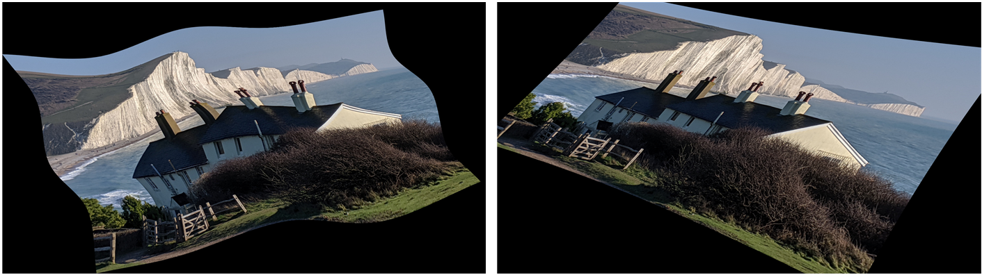
Figure 128. Warp image transform examplesFrom left: arbitrary warp with a 5x5 array of control points, four corner warp with some radial distortion.
Coefficient Tables
Each engine within the Warp IP has read access to its own set of three coefficient tables that define and control the image transform that the IP applies. The three different tables are:
- Mesh coefficients that define the output to input pixel transform
- Fetch coefficients that control the loading of the input image into the cache memory within the engine(s).
- Filter coefficients that control the mapping from the cache memory as the IP generates the interpolated or filtered output pixels.
The format of the mesh coefficients is different to the mesh data that you provide to the software API. The Software API uses 32-bit signed integers for the mesh values; the Warp IP uses a 16-bit offset binary format.
The IP needs just the mesh data to define the warp. The software API uses this mesh data to generate the required coefficient tables.
Warp Mesh Interpolation
The IP defines the warp transform using an 8x8 subsampled mesh. This mesh defines the mapping from the output pixel positions to the corresponding input pixel positions. The 8x8 subsampled mesh requires that only the mappings for the following output pixel positions are defined:
(0,0), (8,0), (16,0) … (W, 0)
(0,8), (8,8), (16,8) … (W, 8)
.
(0,H), (8, H), (16, H) … (W, H)
where W=8*ceil(image width/8) and H=8*ceil(image height/8)
To generate the output pixel positions that lie in between these 8x8 positions, the Warp IP uses bilinear interpolation.
Output Pixel Interpolation and Filtering
The IP generates output pixels with the pixel data from the associated input pixel positions as defined by the warp that the IP applies. The IP generates output pixel values with a bicubic interpolation calculation using a 4x4 kernel of the associated input pixel values.
The weightings for the interpolation over the 4x4 kernel are a combination of a bicubic function and a variable low pass filtering function. The software API automatically applies low pass filtering, which it bases on the amount of downscaling that results for that particular region of the warp.
Blank Skip Regions
When you configure the Warp IP to substantially downscale regions of an image, large areas of the output image can map to points outside the input image. These unmapped regions result in the IP producing black.
Because these regions in the output image do not require any processing of the input image by the Warp IP, for efficiency the IP skips the processing associated with these regions. This skipping process is setup automatically by the software API which determines, from the desired warp mapping, which regions the IP skips. You see this behavior only when Use single memory bounce is off.
Easy Warp
When you turn on Use easy warp:
- The IP supports rotations of 0°, 90°, 180° and 270° and you can apply a horizontal mirror operation before the selected rotation.
- The IP does not configure any engines.
- The IP applies the required rotational or mirrored transform by the video output block as it reads data from external memory.
- The IP does not require any processing engines, giving resource savings and memory bandwidth savings.
For easy warp rotations of 0 or 180°, the maximum input width dimension must not exceed the maximum output width. You set the maximum width with the Maximum output video width parameter. For easy warp rotations of 90° or 270°, the transposing of vertical and horizontal dimensions places restrictions on the input resolution.
| Maximum Output Video Width | Input Height Restriction |
|---|---|
| 2048 | 1088 |
| 3840 | 2176 |
Figure 129. Warp IP block diagram (Easy Warp)
The figure shows a high-level block diagram for the Warp IP with Use Easy warp with its connection to external memory.
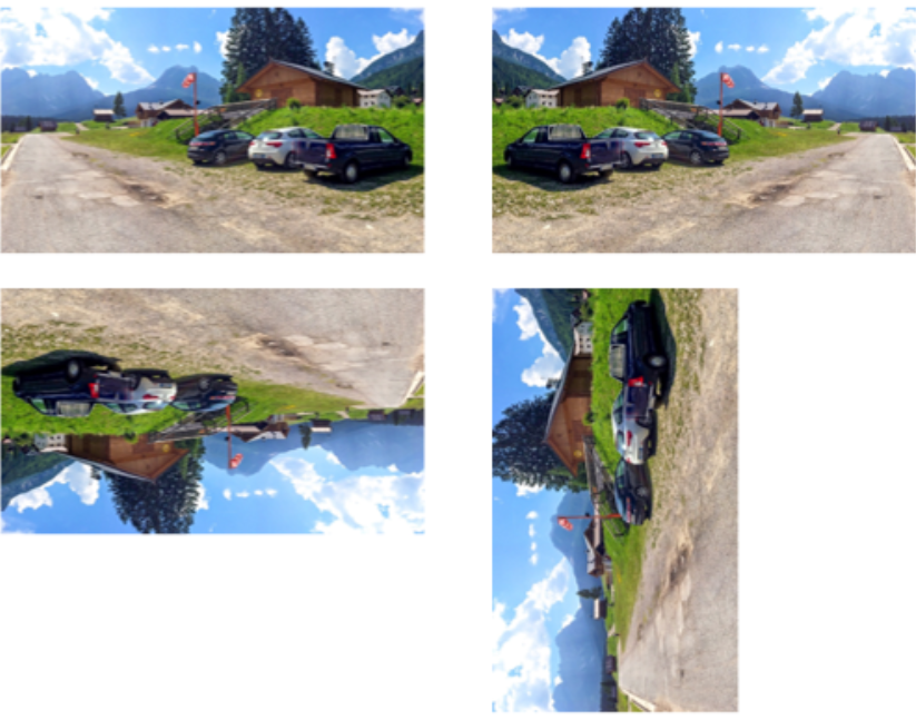
Figure 130. Easy Warp image transform examplesFrom top left clockwise: original image, mirrored, 90° rotate and 180° rotate.
Single Memory Bounce
Generally, turning on Use single memory bounce gives reduced memory bandwidth compared to when it is off. However, single memory bounce may require larger internal RAM. The RAM usage depends on the specific warp transform. For some transforms the IP requires larger amounts of cache. Any increased cache requirement requires increased internal block RAM usage.
With Use single memory bounce on, three cache size options are available: 256, 512 and 1024 cache blocks per engine. With Use single memory bounce off, the IP has a fixed cache size of 256 cache blocks per engine.
Whether you turn on Use single memory bounce depends on the actual transform the IP performs. Intel provides a software tool that determines how much cache the IP needs to process the desired transform. You provide the tool with information such as the input and output resolutions, the transform required, and the number of engines to use. The tool then provides guidance on how much cache to use to process the transform.
For information on the Warp block cache tool, refer to Block Cache Tool. For information on the memory bandwidth implications of running with a single memory bounce, refer to External Memory for Warp IP.
Single Memory Bounce Cache Example
An example of cache usage is given based on a 45 degree rotation with UHD input and output resolutions at 60 fps on an Intel Arria 10 device. This throughput requires that the IP uses two engines.
With Use single memory bounce off, the block RAM usage by the IP is 365 M20Ks.
With Use single memory bounce on, the IP requires 512 cache blocks per engine because of the constraints of the 45 degree rotation. This cache block requirement translates to a block RAM usage of 407 M20Ks.
| Use single memory bounce | Cache blocks per engine | Total block RAM usage |
|---|---|---|
| On | 512 | 407 |
| Off | 256 (fixed) | 365 |