Visible to Intel only — GUID: kly1426141521121
Ixiasoft
1.2.1. Understanding the Different PTP Clocks
1.2.2. Precision Time Protocol (PTP) Synchronization Process
1.2.3. Functional Flow For A 1588 Ordinary Clock Master/Slave Mode System
1.2.4. Functional Flow For A 1588 Transparent Clock Master/Slave Mode System
1.2.5. Functional Flow for A 1588 Boundary Clock Mode System
1.2.6. Timestamp Packet Functional Flow in Linux Driver
Visible to Intel only — GUID: kly1426141521121
Ixiasoft
1.3.2.1.3. Booting Up The Reference Design
- Connect the micro SD card with the bootable image to J5 port on board A.
- Connect USB II blaster cable from Board A to your Windows host that has Arria V SoC development kit installed.
- Turn on the power for Board A to load the bootable image. The Arria V 10GbE appears on the LCD screen on the board when the image is successfully loaded.
- Open the Clock Control application from the Arria V SoC development kit installation on your Windows host.
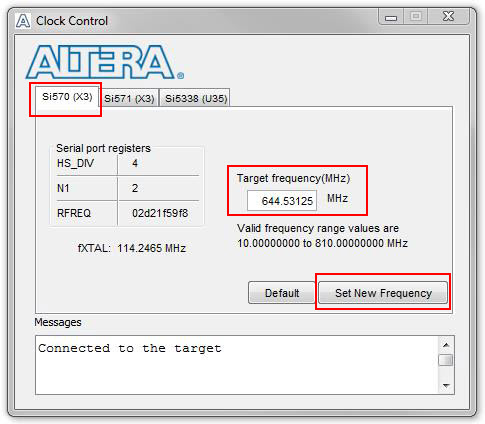
- Set Channel 0 reference clock source, Si570(X3) to 644.53125MHz. This step is required to run the reference design at 10Gbps data rate. FPGA LED [0] will blink every 2 seconds to indicate that the hardware clock is running at 10Gbps data rate if the reference clock source Si570 is successfully configured.
Figure 13. Clock Control Application Settings
- You may choose to access the Linux operating system on the Arria V SoC development board using any serial communication program such as Putty or minicom applications that are available to you. In these steps, Putty application is used as an example. You may follow the setup shown in the following figure to configure the Putty tool.
Figure 14. Putty Configuration Settings
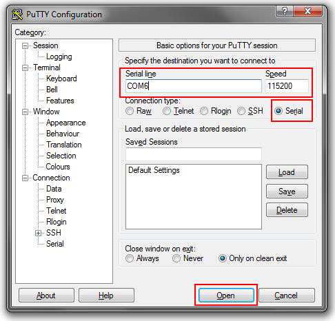 Note: Always check the serial line ID of the COM port connected to your computer. In this example, the serial line ID is COM6.
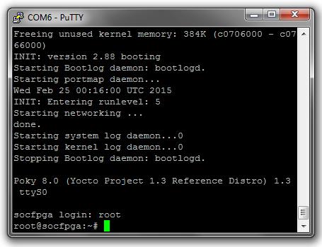
 - Type root as the login name when requested.
Figure 15. Arria V SoC Operating System Login Prompt
- Repeat step 1 to step 8 for Board B.
- In the Putty console, type reboot to reset the system for both Board A and Board B.
- Observe that FPGA LED [2] on board A and board B will turn off for sometime before turning on again indicating that the link between Board A and Board B is successfully connected.
- You may connect port J15 to an oscilloscope in order to view the ToD Pulse Per Second waveform.