Visible to Intel only — GUID: kly1426138738186
Ixiasoft
1.2.1. Understanding the Different PTP Clocks
1.2.2. Precision Time Protocol (PTP) Synchronization Process
1.2.3. Functional Flow For A 1588 Ordinary Clock Master/Slave Mode System
1.2.4. Functional Flow For A 1588 Transparent Clock Master/Slave Mode System
1.2.5. Functional Flow for A 1588 Boundary Clock Mode System
1.2.6. Timestamp Packet Functional Flow in Linux Driver
Visible to Intel only — GUID: kly1426138738186
Ixiasoft
1.3.2.1.2. Setting Up Development Kit
The following procedures are performed using a Windows host.
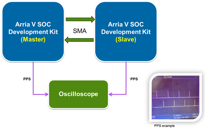
The figure below shows the hardware connections in order to run this reference design.
Figure 11. Reference Design Hardware Setup
- Download and install Quartus II Subscription Edition software v14.1 and Altera Arria V SoC Development Kit Installations on your Windows host.
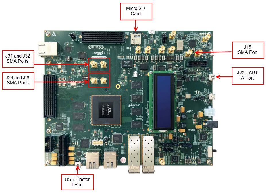
- Place two Arria V SoC development boards (5ASTFD5K3F40I3NES) side by side. In the following steps, the two Arria V SoC development boards will be referred to as Board A and Board B. Setup the SMA connections between these 2 boards per below:
- Port J24 on Board A connects to port J31 on Board B.
- Port J25 on Board A connects to port J32 on Board B.
- Port J24 on Board B connects to port J31 on Board A.
- Port J25 on Board B connects to port J32 on Board A.
Note: Refer to Arria V SoC Development Board Reference Manual for more information on connectors available on the board. - Set MSEL [4..0] pins (SW3) to value 00110 to enable compression feature for Board A and Board B.
- Connect both serial cables on Board A and Board B (J22 port) to your Windows host.
Figure 12. Arria V SoC Development Board Connections Overview