3.1. Board Overview
This section provides an overview of the evaluation kit, including an annotated board image and component descriptions.
Figure 3. Intel® MAX® 10 FPGA 10M50 Evaluation Kit Features - Board Image (Front View)—EK-10M50F484 (Power Solution 1)
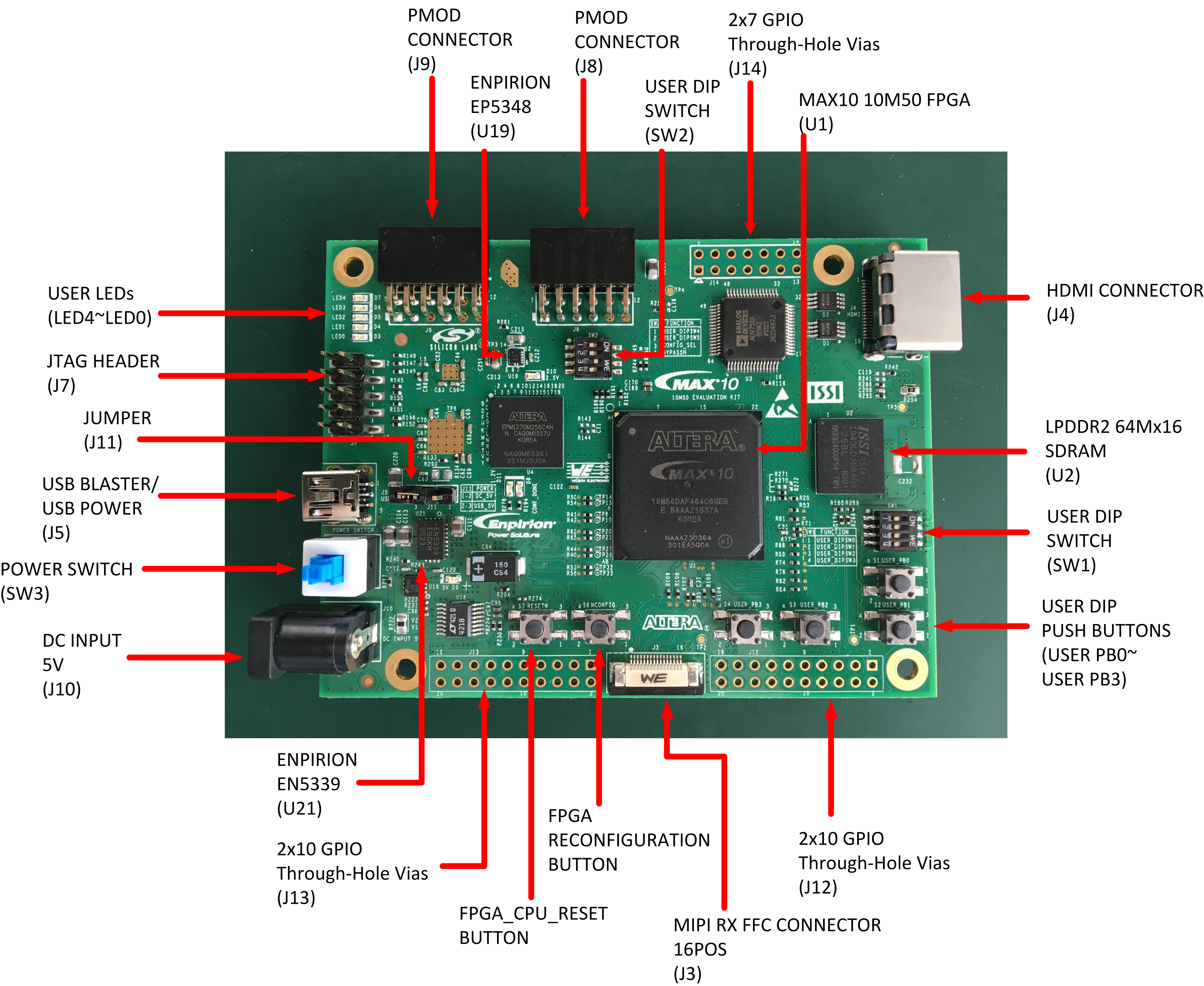
Figure 4. Intel® MAX® 10 FPGA 10M50 Evaluation Kit Features - Board Image (Rear View)—EK-10M50F484 (Power Solution 1)
Figure 5. Intel® MAX® 10 FPGA 10M50 Evaluation Kit Features - Board Image (Front View)—DK-DEV-10M50F484-C (Power Solution 2)
Figure 6. Intel® MAX® 10 FPGA 10M50 Evaluation Kit Features - Board Image (Rear View)—DK-DEV-10M50F484-C (Power Solution 2)
| Board Reference | Type | Description |
|---|---|---|
| Featured Device—Power Solution 1 | ||
| U1 | FPGA | Intel® MAX® 10 FPGA 10M50DAF484C6GES, 50K LEs, F484 package, -6ES speed grade. |
| U13 | CPLD | MAX® II EPM1270 256-MBGA, 2.5V/3.3V, VCCINT for on-board Intel® FPGA Download Cable II. |
| U17 | Power Regulator | Enpirion EN5329QI 2A PowerSoC low profile synchronous buck DC-DC converter with integrated inductor. |
| U19, U22 | Power Regulator | Enpirion EP5348UI 400mA PowerSoC synchronous buck regulator with integrated inductor. |
| U20 | Power Regulator | Enpirion EP5358HUI 600mA PowerSoC synchronous buck regulator with integrated inductor. |
| U21 | Power Regulator | Enpirion EN5339QI 3A PowerSoC low profile synchronous buck DC-DC converter with integrated inductor. |
| Featured Device—Power Solution 2 | ||
| U1 | FPGA | Intel® MAX® 10 FPGA 10M50DAF484C6GES, 50K LEs, F484 package, -6ES speed grade. |
| U13 | CPLD | MAX® II EPM1270 256-MBGA, 2.5V/3.3V, VCCINT for on-board Intel® FPGA Download Cable II. |
| U17, U21 | Power Regulator | MPS MPM3632SGPQ-C879-Z 3A synchronous buck DC-DC converter with integrated inductor. |
| U19, U20, U22 | Power Regulator | MPS MPM3804GG-C879-Z 600mA synchronous buck regulator with integrated inductor. |
| Configuration and Setup Elements | ||
| J5 | On-Board (Embedded) Intel® FPGA Download Cable II | Mini Type-B USB connector for programming and debugging the FPGA. |
| J7 | 10-pin header | Optional JTAG direct via 10-pin header for external download cables. |
| SW2 | DIP configuration and user switch | SW2 includes switches to control boot images and JTAG bypass. |
| S6 | MAX10 nCONFIG push button | Toggling this button causes the FPGA to reconfigure from on-die Configuration Flash Memory (CFM). |
| S7 | FPGA register push button | Toggling this button resets all registers in the FPGA. |
| J11 | Jumper for board power option | Default connection is Pins 2 and 3 position, which uses USB power supply. If needed, change jumper position to Pins 1 and 2 for DC adapter power supply solution. |
| Status Elements | ||
| D8 | Configuration done LED, green | Illuminates when the FPGA is configured. |
| D9 | Power LED, yellow | Indicates that 5V is powered up successfully. |
| D10 | Power LED, yellow | Indicates that 2.5V is powered up successfully. |
| D11 | Power LED, yellow | Indicates that 1.2V is powered up successfully. |
| Clock Circuitry | ||
| U14 | Programmable Clock | Four channel programmable oscillator with default frequencies of 24, 24, 125,100 MHz. |
| U15 | 50-MHz oscillator | 50-MHz crystal oscillator for general purpose logic of Intel® MAX® 10 and MAX II devices. |
| General User Input and Output | ||
| S1, S2, S3, S4 | User push buttons | Four user push buttons. Driven low when pressed. |
| D3, D4, D5, D6, D7 | User LEDs, green | Five user LEDs. Illuminate when driven low. |
| SW1, SW2.1, SW2.2 | User DIP switches | Quad user DIP switches. |
| Memory Devices | ||
| U2 | LPDDR2 SDRAM memory | 64 M x16 |
| U23 | Quad serial peripheral interface (quad SPI) flash | 512 Mb |
| Video and Display Ports | ||
| J1 | MIPI CSI-2 transmitter output | MIPI CSI-2 transmitter output to Leopard Imaging LI-MIPI-USB3-Tester module. |
| J2 | MIPI CSI-2 receiver | MIPI CSI-2 receiver input from Leopard Imaging LI-CAM-OV10640-MIPI module. |
| J3 | MIPI CSI-2 receiver | MIPI CSI-2 receiver input from UDOO Camera Module OV5640. |
| J4 | HDMI video output | 19-pin HDMI connector which provides a HDMIv1.4 video output of up to 1080p through an ADI (Analog Devices, Inc) HDMI transmitter (ADV7513). |
| I/O and Expansion Ports | ||
| J8, J9 | Two Diligent Pmod connectors | 12-pin interface with 8 I/O signal pins used to connect low frequency, low I/O peripheral modules. |
| J12, J13 | Two 2x10 GPIO connectors, user install | You can use this area to connect or solder additional components for connection of 9 true LVDS pairs with clock input and output, or 22 single-ended I/O signals. |
| J14 | 2x7 GPIO connectors, user install | You can use this area to connect or solder additional components for connection of 10 single-ended I/O signals. |
| Power Supply | ||
| J10 | DC input jack | Accepts 5V DC power supply when USB power supply is not in use. |
| SW3 | Power switch | When using DC power adapter, switch to power on or off the board when power is supplied from the DC input jack. DC adapter and USB power don't work at the same time. |
| J5 | USB connector | USB power supply. Use with USB Y cable to provide 1A current. DC adapter power and USB power don't work at the same time. |