Visible to Intel only — GUID: pde1436981280625
Ixiasoft
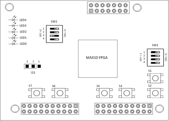
2.4. Factory Default Switch and Jumper Settings
Figure 2. Switch Locations and Default Settings (Board Top)
| Board Reference | Signal Name | Function | Default Position |
|---|---|---|---|
| SW1.1 | USER_DIPSW0 | User-Defined | HIGH (OFF =1) |
| SW1.2 | USER_DIPSW1 | User-Defined | HIGH (OFF =1) |
| SW1.3 | USER_DIPSW2 | User-Defined | HIGH (OFF =1) |
| SW1.4 | USER_DIPSW3 | User-Defined | HIGH (OFF =1) |
| Board Reference | Signal Name | Function | Default Position |
|---|---|---|---|
| SW2.1 | USER_DIPSW4 | User-Defined | HIGH (OFF =1) |
| SW2.2 | USER_DIPSW5 | User-Defined | HIGH (OFF =1) |
| SW2.3 | CONFIG_SEL | CONFIG_SEL: Use this pin to choose CFM0, CFM1 or CFM2 image as the first boot image in dual-image configuration. If the CONFIG_SEL is set to low, the first boot image is CFM0 image. If CONFIG_SEL is set o high, the first boot image is CFM1 or CFM2 image. This pin is read before user mode and before the nSTATUS pin is asserted. | LOW (ON =0) |
| SW2.4 | VTAP_BYPASSn | A virtual JTAG device is provided within the on-board Intel® FPGA Download Cable II, it provides access to diagnostic hardware and board identification information. The device shows up as an extra device on the JTAG chain with ID: 020D10DD. This switch removes the virtual JTAG device from the JTAG chain. | HIGH (OFF =1) |
| Jumper | Function | Setting |
|---|---|---|
| J11[1-2] | Jumper for board DC adapter power option when R292 and R293 not installed | Pins 1 and 2 |
| J11[2-3] | Jumper for board USB power option when R292 and R293 not installed. This is the default power jumper position. | Pins 2 and 3 |