Visible to Intel only — GUID: hco1416491777356
Ixiasoft
1. Release Information
2. External Memory Interfaces Arria® 10 FPGA IP Introduction
3. Arria® 10 EMIF IP Product Architecture
4. Arria® 10 EMIF IP End-User Signals
5. Arria® 10 EMIF – Simulating Memory IP
6. Arria® 10 EMIF IP for DDR3
7. Arria® 10 EMIF IP for DDR4
8. Arria® 10 EMIF IP for QDR II/II+/II+ Xtreme
9. Arria® 10 EMIF IP for QDR-IV
10. Arria® 10 EMIF IP for RLDRAM 3
11. Arria® 10 EMIF IP for LPDDR3
12. Arria® 10 EMIF IP Timing Closure
13. Optimizing Controller Performance
14. Arria® 10 EMIF IP Debugging
15. External Memory Interfaces Arria® 10 FPGA IP User Guide Archives
16. Document Revision History for External Memory Interfaces Arria® 10 FPGA IP User Guide
3.1. EMIF Architecture: Introduction
3.2. Arria® 10 EMIF Sequencer
3.3. Arria® 10 EMIF Calibration
3.4. Periodic OCT Recalibration
3.5. Arria® 10 EMIF Controller
3.6. Hardware Resource Sharing Among Multiple EMIFs
3.7. Arria® 10 EMIF for Hard Processor Subsystem
3.8. Arria® 10 EMIF Ping Pong PHY
3.9. Arria® 10 EMIF and SmartVID
4.1.1. Intel Arria 10 EMIF IP Interfaces for DDR3
4.1.2. Intel Arria 10 EMIF IP Interfaces for DDR4
4.1.3. Intel Arria 10 EMIF IP Interfaces for LPDDR3
4.1.4. Intel Arria 10 EMIF IP Interfaces for QDR II/II+/II+ Xtreme
4.1.5. Intel Arria 10 EMIF IP Interfaces for QDR-IV
4.1.6. Intel Arria 10 EMIF IP Interfaces for RLDRAM 3
4.1.1.1. pll_ref_clk for DDR3
4.1.1.2. pll_locked for DDR3
4.1.1.3. pll_extra_clk_0 for DDR3
4.1.1.4. pll_extra_clk_1 for DDR3
4.1.1.5. pll_extra_clk_2 for DDR3
4.1.1.6. pll_extra_clk_3 for DDR3
4.1.1.7. oct for DDR3
4.1.1.8. mem for DDR3
4.1.1.9. status for DDR3
4.1.1.10. afi_reset_n for DDR3
4.1.1.11. afi_clk for DDR3
4.1.1.12. afi_half_clk for DDR3
4.1.1.13. afi for DDR3
4.1.1.14. emif_usr_reset_n for DDR3
4.1.1.15. emif_usr_clk for DDR3
4.1.1.16. emif_usr_reset_n_sec for DDR3
4.1.1.17. emif_usr_clk_sec for DDR3
4.1.1.18. cal_debug_reset_n for DDR3
4.1.1.19. cal_debug_clk for DDR3
4.1.1.20. cal_debug_out_reset_n for DDR3
4.1.1.21. cal_debug_out_clk for DDR3
4.1.1.22. clks_sharing_master_out for DDR3
4.1.1.23. clks_sharing_slave_in for DDR3
4.1.1.24. clks_sharing_slave_out for DDR3
4.1.1.25. ctrl_amm for DDR3
4.1.1.26. ctrl_auto_precharge for DDR3
4.1.1.27. ctrl_user_priority for DDR3
4.1.1.28. ctrl_ecc_user_interrupt for DDR3
4.1.1.29. ctrl_ecc_readdataerror for DDR3
4.1.1.30. ctrl_mmr_slave for DDR3
4.1.1.31. hps_emif for DDR3
4.1.1.32. cal_debug for DDR3
4.1.1.33. cal_debug_out for DDR3
4.1.2.1. pll_ref_clk for DDR4
4.1.2.2. pll_locked for DDR4
4.1.2.3. pll_extra_clk_0 for DDR4
4.1.2.4. pll_extra_clk_1 for DDR4
4.1.2.5. pll_extra_clk_2 for DDR4
4.1.2.6. pll_extra_clk_3 for DDR4
4.1.2.7. oct for DDR4
4.1.2.8. mem for DDR4
4.1.2.9. status for DDR4
4.1.2.10. afi_reset_n for DDR4
4.1.2.11. afi_clk for DDR4
4.1.2.12. afi_half_clk for DDR4
4.1.2.13. afi for DDR4
4.1.2.14. emif_usr_reset_n for DDR4
4.1.2.15. emif_usr_clk for DDR4
4.1.2.16. emif_usr_reset_n_sec for DDR4
4.1.2.17. emif_usr_clk_sec for DDR4
4.1.2.18. cal_debug_reset_n for DDR4
4.1.2.19. cal_debug_clk for DDR4
4.1.2.20. cal_debug_out_reset_n for DDR4
4.1.2.21. cal_debug_out_clk for DDR4
4.1.2.22. clks_sharing_master_out for DDR4
4.1.2.23. clks_sharing_slave_in for DDR4
4.1.2.24. clks_sharing_slave_out for DDR4
4.1.2.25. ctrl_amm for DDR4
4.1.2.26. ctrl_auto_precharge for DDR4
4.1.2.27. ctrl_user_priority for DDR4
4.1.2.28. ctrl_ecc_user_interrupt for DDR4
4.1.2.29. ctrl_ecc_readdataerror for DDR4
4.1.2.30. ctrl_mmr_slave for DDR4
4.1.2.31. hps_emif for DDR4
4.1.2.32. cal_debug for DDR4
4.1.2.33. cal_debug_out for DDR4
4.1.3.1. pll_ref_clk for LPDDR3
4.1.3.2. pll_locked for LPDDR3
4.1.3.3. pll_extra_clk_0 for LPDDR3
4.1.3.4. pll_extra_clk_1 for LPDDR3
4.1.3.5. pll_extra_clk_2 for LPDDR3
4.1.3.6. pll_extra_clk_3 for LPDDR3
4.1.3.7. oct for LPDDR3
4.1.3.8. mem for LPDDR3
4.1.3.9. status for LPDDR3
4.1.3.10. afi_reset_n for LPDDR3
4.1.3.11. afi_clk for LPDDR3
4.1.3.12. afi_half_clk for LPDDR3
4.1.3.13. afi for LPDDR3
4.1.3.14. emif_usr_reset_n for LPDDR3
4.1.3.15. emif_usr_clk for LPDDR3
4.1.3.16. cal_debug_reset_n for LPDDR3
4.1.3.17. cal_debug_clk for LPDDR3
4.1.3.18. cal_debug_out_reset_n for LPDDR3
4.1.3.19. cal_debug_out_clk for LPDDR3
4.1.3.20. clks_sharing_master_out for LPDDR3
4.1.3.21. clks_sharing_slave_in for LPDDR3
4.1.3.22. clks_sharing_slave_out for LPDDR3
4.1.3.23. ctrl_user_priority for LPDDR3
4.1.3.24. ctrl_mmr_slave for LPDDR3
4.1.3.25. cal_debug for LPDDR3
4.1.3.26. cal_debug_out for LPDDR3
4.1.4.1. pll_ref_clk for QDR II/II+/II+ Xtreme
4.1.4.2. pll_locked for QDR II/II+/II+ Xtreme
4.1.4.3. pll_extra_clk_0 for QDR II/II+/II+ Xtreme
4.1.4.4. pll_extra_clk_1 for QDR II/II+/II+ Xtreme
4.1.4.5. pll_extra_clk_2 for QDR II/II+/II+ Xtreme
4.1.4.6. pll_extra_clk_3 for QDR II/II+/II+ Xtreme
4.1.4.7. oct for QDR II/II+/II+ Xtreme
4.1.4.8. mem for QDR II/II+/II+ Xtreme
4.1.4.9. status for QDR II/II+/II+ Xtreme
4.1.4.10. emif_usr_reset_n for QDR II/II+/II+ Xtreme
4.1.4.11. emif_usr_clk for QDR II/II+/II+ Xtreme
4.1.4.12. cal_debug_reset_n for QDR II/II+/II+ Xtreme
4.1.4.13. cal_debug_clk for QDR II/II+/II+ Xtreme
4.1.4.14. cal_debug_out_reset_n for QDR II/II+/II+ Xtreme
4.1.4.15. cal_debug_out_clk for QDR II/II+/II+ Xtreme
4.1.4.16. clks_sharing_master_out for QDR II/II+/II+ Xtreme
4.1.4.17. clks_sharing_slave_in for QDR II/II+/II+ Xtreme
4.1.4.18. clks_sharing_slave_out for QDR II/II+/II+ Xtreme
4.1.4.19. ctrl_amm for QDR II/II+/II+ Xtreme
4.1.4.20. cal_debug for QDR II/II+/II+ Xtreme
4.1.4.21. cal_debug_out for QDR II/II+/II+ Xtreme
4.1.5.1. pll_ref_clk for QDR-IV
4.1.5.2. pll_locked for QDR-IV
4.1.5.3. pll_extra_clk_0 for QDR-IV
4.1.5.4. pll_extra_clk_1 for QDR-IV
4.1.5.5. pll_extra_clk_2 for QDR-IV
4.1.5.6. pll_extra_clk_3 for QDR-IV
4.1.5.7. oct for QDR-IV
4.1.5.8. mem for QDR-IV
4.1.5.9. status for QDR-IV
4.1.5.10. afi_reset_n for QDR-IV
4.1.5.11. afi_clk for QDR-IV
4.1.5.12. afi_half_clk for QDR-IV
4.1.5.13. afi for QDR-IV
4.1.5.14. emif_usr_reset_n for QDR-IV
4.1.5.15. emif_usr_clk for QDR-IV
4.1.5.16. cal_debug_reset_n for QDR-IV
4.1.5.17. cal_debug_clk for QDR-IV
4.1.5.18. cal_debug_out_reset_n for QDR-IV
4.1.5.19. cal_debug_out_clk for QDR-IV
4.1.5.20. clks_sharing_master_out for QDR-IV
4.1.5.21. clks_sharing_slave_in for QDR-IV
4.1.5.22. clks_sharing_slave_out for QDR-IV
4.1.5.23. ctrl_amm for QDR-IV
4.1.5.24. cal_debug for QDR-IV
4.1.5.25. cal_debug_out for QDR-IV
4.1.6.1. pll_ref_clk for RLDRAM 3
4.1.6.2. pll_locked for RLDRAM 3
4.1.6.3. pll_extra_clk_0 for RLDRAM 3
4.1.6.4. pll_extra_clk_1 for RLDRAM 3
4.1.6.5. pll_extra_clk_2 for RLDRAM 3
4.1.6.6. pll_extra_clk_3 for RLDRAM 3
4.1.6.7. oct for RLDRAM 3
4.1.6.8. mem for RLDRAM 3
4.1.6.9. status for RLDRAM 3
4.1.6.10. afi_reset_n for RLDRAM 3
4.1.6.11. afi_clk for RLDRAM 3
4.1.6.12. afi_half_clk for RLDRAM 3
4.1.6.13. afi for RLDRAM 3
4.1.6.14. cal_debug_reset_n for RLDRAM 3
4.1.6.15. cal_debug_clk for RLDRAM 3
4.1.6.16. cal_debug_out_reset_n for RLDRAM 3
4.1.6.17. cal_debug_out_clk for RLDRAM 3
4.1.6.18. clks_sharing_master_out for RLDRAM 3
4.1.6.19. clks_sharing_slave_in for RLDRAM 3
4.1.6.20. clks_sharing_slave_out for RLDRAM 3
4.1.6.21. cal_debug for RLDRAM 3
4.1.6.22. cal_debug_out for RLDRAM 3
4.4.1. ctrlcfg0
4.4.2. ctrlcfg1
4.4.3. dramtiming0
4.4.4. sbcfg1
4.4.5. caltiming0
4.4.6. caltiming1
4.4.7. caltiming2
4.4.8. caltiming3
4.4.9. caltiming4
4.4.10. caltiming9
4.4.11. dramaddrw
4.4.12. sideband0
4.4.13. sideband1
4.4.14. sideband2
4.4.15. sideband3
4.4.16. sideband4
4.4.17. sideband5
4.4.18. sideband6
4.4.19. sideband7
4.4.20. sideband8
4.4.21. sideband9
4.4.22. sideband10
4.4.23. sideband11
4.4.24. sideband12
4.4.25. sideband13
4.4.26. dramsts
4.4.27. niosreserve0
4.4.28. niosreserve1
4.4.29. ecc3: ECC Error and Interrupt Configuration
4.4.30. ecc4: Status and Error Information
4.4.31. ecc5: Address of Most Recent SBE/DBE
4.4.32. ecc6: Address of Most Recent Correction Command Dropped
6.1.1. Intel Arria 10 EMIF IP DDR3 Parameters: General
6.1.2. Intel Arria 10 EMIF IP DDR3 Parameters: Memory
6.1.3. Intel Arria 10 EMIF IP DDR3 Parameters: Mem I/O
6.1.4. Intel Arria 10 EMIF IP DDR3 Parameters: FPGA I/O
6.1.5. Intel Arria 10 EMIF IP DDR3 Parameters: Mem Timing
6.1.6. Intel Arria 10 EMIF IP DDR3 Parameters: Board
6.1.7. Intel Arria 10 EMIF IP DDR3 Parameters: Controller
6.1.8. Intel Arria 10 EMIF IP DDR3 Parameters: Diagnostics
6.1.9. Intel Arria 10 EMIF IP DDR3 Parameters: Example Designs
7.1.1. Intel Arria 10 EMIF IP DDR4 Parameters: General
7.1.2. Intel Arria 10 EMIF IP DDR4 Parameters: Memory
7.1.3. Intel Arria 10 EMIF IP DDR4 Parameters: Mem I/O
7.1.4. Intel Arria 10 EMIF IP DDR4 Parameters: FPGA I/O
7.1.5. Intel Arria 10 EMIF IP DDR4 Parameters: Mem Timing
7.1.6. Intel Arria 10 EMIF IP DDR4 Parameters: Board
7.1.7. Intel Arria 10 EMIF IP DDR4 Parameters: Controller
7.1.8. Intel Arria 10 EMIF IP DDR4 Parameters: Diagnostics
7.1.9. Intel Arria 10 EMIF IP DDR4 Parameters: Example Designs
7.4.4.1. General Layout Guidelines
7.4.4.2. Layout Guidelines
7.4.4.3. Length Matching Rules
7.4.4.4. Spacing Guidelines
7.4.4.5. Layout Guidelines for DDR3 and DDR4 SDRAM Wide Interface (>72 bits)
7.4.4.6. Fly-By Network Design for Clock, Command, and Address Signals
7.4.4.7. Additional Layout Guidelines for DDR4 Twin-die Devices
8.1.1. Intel Arria 10 EMIF IP QDR II/II+/II+ Xtreme Parameters: General
8.1.2. Intel Arria 10 EMIF IP QDR II/II+/II+ Xtreme Parameters: Memory
8.1.3. Intel Arria 10 EMIF IP QDR II/II+/II+ Xtreme Parameters: FPGA I/O
8.1.4. Intel Arria 10 EMIF IP QDR II/II+/II+ Xtreme Parameters: Mem Timing
8.1.5. Intel Arria 10 EMIF IP QDR II/II+/II+ Xtreme Parameters: Board
8.1.6. Intel Arria 10 EMIF IP QDR II/II+/II+ Xtreme Parameters: Controller
8.1.7. Intel Arria 10 EMIF IP QDR II/II+/II+ Xtreme Parameters: Diagnostics
8.1.8. Intel Arria 10 EMIF IP QDR II/II+/II+ Xtreme Parameters: Example Designs
8.3.1.6.1. General Guidelines
8.3.1.6.2. QDR II, QDR II+ and QDR II+ Xtreme SRAM Command Signals
8.3.1.6.3. QDR II, QDR II+ and QDR II+ Xtreme SRAM Address Signals
8.3.1.6.4. QDR II, QDR II+, and QDR II+ Xtreme SRAM Clock Signals
8.3.1.6.5. QDR II, QDR II+ and QDR II+ Xtreme SRAM Data, BWS, and QVLD Signals
8.3.1.6.6. Resource Sharing Guidelines (Multiple Interfaces)
9.1.1. Intel Arria 10 EMIF IP QDR-IV Parameters: General
9.1.2. Intel Arria 10 EMIF IP QDR-IV Parameters: Memory
9.1.3. Intel Arria 10 EMIF IP QDR-IV Parameters: FPGA I/O
9.1.4. Intel Arria 10 EMIF IP QDR-IV Parameters: Mem Timing
9.1.5. Intel Arria 10 EMIF IP QDR-IV Parameters: Board
9.1.6. Intel Arria 10 EMIF IP QDR-IV Parameters: Controller
9.1.7. Intel Arria 10 EMIF IP QDR-IV Parameters: Diagnostics
9.1.8. Intel Arria 10 EMIF IP QDR-IV Parameters: Example Designs
10.1.1. Intel Arria 10 EMIF IP RLDRAM 3 Parameters: General
10.1.2. Intel Arria 10 EMIF IP RLDRAM 3 Parameters: Memory
10.1.3. Intel Arria 10 EMIF IP RLDRAM 3 Parameters: FPGA I/O
10.1.4. Intel Arria 10 EMIF IP RLDRAM 3 Parameters: Mem Timing
10.1.5. Intel Arria 10 EMIF IP RLDRAM 3 Parameters: Board
10.1.6. Intel Arria 10 EMIF IP RLDRAM 3 Parameters: Controller
10.1.7. Intel Arria 10 EMIF IP RLDRAM 3 Parameters: Diagnostics
10.1.8. Intel Arria 10 EMIF IP RLDRAM 3 Parameters: Example Designs
11.1.1. Intel Arria 10 EMIF IP LPDDR3 Parameters: General
11.1.2. Intel Arria 10 EMIF IP LPDDR3 Parameters: Memory
11.1.3. Intel Arria 10 EMIF IP LPDDR3 Parameters: Mem I/O
11.1.4. Intel Arria 10 EMIF IP LPDDR3 Parameters: FPGA I/O
11.1.5. Intel Arria 10 EMIF IP LPDDR3 Parameters: Mem Timing
11.1.6. Intel Arria 10 EMIF IP LPDDR3 Parameters: Board
11.1.7. Intel Arria 10 EMIF IP LPDDR3 Parameters: Controller
11.1.8. Intel Arria 10 EMIF IP LPDDR3 Parameters: Diagnostics
11.1.9. Intel Arria 10 EMIF IP LPDDR3 Parameters: Example Designs
13.4.1. Auto-Precharge Commands
13.4.2. Latency
13.4.3. Calibration
13.4.4. Bank Interleaving
13.4.5. Additive Latency and Bank Interleaving
13.4.6. User-Controlled Refresh
13.4.7. Frequency of Operation
13.4.8. Series of Reads or Writes
13.4.9. Data Reordering
13.4.10. Starvation Control
13.4.11. Command Reordering
13.4.12. Bandwidth
13.4.13. Enable Command Priority Control
14.1. Interface Configuration Performance Issues
14.2. Functional Issue Evaluation
14.3. Timing Issue Characteristics
14.4. Verifying Memory IP Using the Signal Tap II Logic Analyzer
14.5. Hardware Debugging Guidelines
14.6. Categorizing Hardware Issues
14.7. Debugging Arria® 10 EMIF IP
14.8. Using the Traffic Generator with the Generated Design Example
14.5.1. Create a Simplified Design that Demonstrates the Same Issue
14.5.2. Measure Power Distribution Network
14.5.3. Measure Signal Integrity and Setup and Hold Margin
14.5.4. Vary Voltage
14.5.5. Operate at a Lower Speed
14.5.6. Determine Whether the Issue Exists in Previous Versions of Software
14.5.7. Determine Whether the Issue Exists in the Current Version of Software
14.5.8. Try A Different PCB
14.5.9. Try Other Configurations
14.5.10. Debugging Checklist
14.7.1.1. User Interface
14.7.1.2. Communication
14.7.1.3. Setup and Use
14.7.1.4. Configuring Your EMIF IP for Use with the Debug Toolkit
14.7.1.5. Reports
14.7.1.6. On-Die Termination Calibration
14.7.1.7. Eye Diagram
14.7.1.8. Driver Margining for Arria® 10 EMIF IP
14.7.1.9. Example Tcl Script for Running the EMIF Debug Toolkit
14.7.1.10. Using the EMIF Debug Toolkit with Arria® 10 HPS Interfaces
Visible to Intel only — GUID: hco1416491777356
Ixiasoft
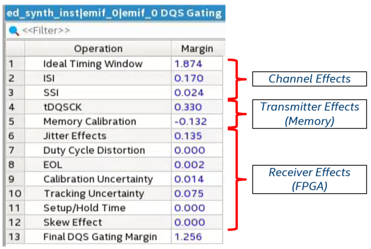
12.1.1.2.4. DQS Gating / Postamble
Postamble timing is a setup period during which the DQS signal goes low after all the DQ data has been received from the memory device during a read operation. After postamble time, the DQS signal returns from a low-impedance to a high-impedance state to disable DQS and disallow any glitches from writing false data over valid data.
The Timing Analyzer analyzes the postamble timing path in DDRx memory protocols only through an equation which considers memory calibration, calibration uncertainty, and tracking uncertainties as shown in the following figure.
Figure 101. DQS Gating Timing Analysis