Visible to Intel only — GUID: hdf1468416503654
Ixiasoft
1. About the Drive-On-Chip Design Example for Intel® MAX® 10 Devices
2. Features of the Drive-on-Chip Design Example for Intel® MAX® 10 Devices
3. Getting Started with the Drive-On-Chip Design Example for Intel® MAX® 10 Devices
4. Rebuilding the Drive-On-Chip Design Example for Intel® MAX® 10 Devices
5. About the Scaling of Feedback Signals
6. Motor Control Software
7. Functional Description of the Drive-on-Chip Design Example
8. Achieving Timing Closure on a Motor Control Design
9. Design Security Recommendations
10. Reference Documents for the Drive-on-Chip Design Example
11. Document Revision History for AN 773: Drive-on-Chip Design Example for Intel® MAX® 10 Devices
3.1. Software Requirements for the Drive-On-Chip Design Example for Intel® MAX® 10 Devices
3.2. Hardware Requirements for the Drive-On-Chip Design Example for Intel® MAX® 10 Devices
3.3. Downloading and Installing the Design
3.4. Setting Up the Motor Control Board with your Development Board for the Drive-On-Chip Design Example for Intel® MAX® 10 Devices
3.5. Importing the Drive-On-Chip Design Example Software Project
3.6. Configuring the FPGA Hardware for the Drive-On-Chip Design Example for Intel® MAX® 10 Devices
3.7. Programming the Nios II Software to the Device for the Drive-On-Chip Design Example for Intel® MAX® 10 Devices
3.8. Applying Power to the Power Board
3.9. Debugging and Monitoring the Drive-On-Chip Design Example with System Console
3.10. System Console GUI Upper Pane for the Drive-On-Chip Design Example
3.11. System Console GUI Lower Pane for the Drive-On-Chip Design Example
3.12. Controlling the DC-DC Converter
3.13. Tuning the PI Controller Gains
3.14. Controlling the Speed and Position Demonstrations
3.15. Monitoring Performance
4.1. Changing the Intel® MAX® 10 ADC Thresholds or Conversion Sequence
4.2. Generating the Qsys System
4.3. Compiling the Hardware in the Intel Quartus Prime Software
4.4. Generating and Building the Nios II BSP for the Drive-On-Chip Design Example
4.5. Software Application Configuration Files
4.6. Compiling the Software Application for the Drive-On-Chip Design Example
4.7. Programming the Design into Flash Memory
7.1. Processor Subsystem
7.2. Six-channel PWM Interface
7.3. DC Link Monitor
7.4. Drive System Monitor
7.5. Quadrature Encoder Interface
7.6. Sigma-Delta ADC Interface for Drive Axes
7.7. Intel® MAX® 10 ADCs
7.8. ADC Threshold Sink
7.9. DC-DC Converter
7.10. Motor Control Modes
7.11. FOC Subsystem
7.12. DEKF Technique
7.13. Signals
7.14. Registers
7.11.1. DSP Builder for Intel FPGAs Model for the Drive-on-Chip Designs
7.11.2. Avalon Memory-Mapped Interface
7.11.3. About DSP Builder for Intel FPGAs
7.11.4. DSP Builder for Intel FPGAs Folding
7.11.5. DSP Builder for Intel FPGAs Model Resource Usage
7.11.6. DSP Builder for Intel FPGAs Design Guidelines
7.11.7. Generating VHDL for the DSP Builder Models for the Drive-on-Chip Designs
Visible to Intel only — GUID: hdf1468416503654
Ixiasoft
7. Functional Description of the Drive-on-Chip Design Example
The design consists of two main elements: Qsys, DSP Builder for Intel FPGAs, IP, and RTL sources compiled into an FPGA programming file; and C source code compiled to run on a Nios II processor in the FPGA.
The Qsys system consists of:
- Processor subsystem
- DC link monitors
- Intel® MAX® 10 modular dual ADC
- DC-DC converter
- FOC subsystem
- One or two motor drive axes comprising the following motor control peripheral components:
- 6-channel PWM
- Drive system monitor
- Quadrature encoder interface
- Resolver SPI interface
- ADC interface
Figure 22. Qsys System Top-Level Design
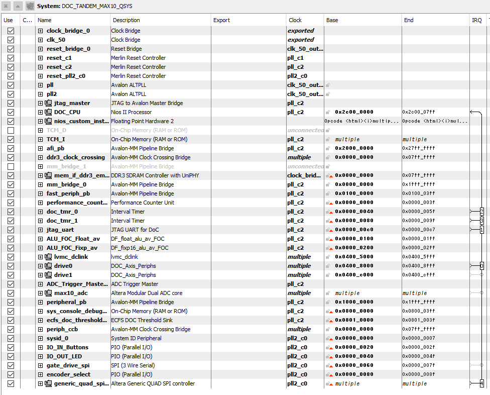
Figure 23. Qsys System for a Drive Axis
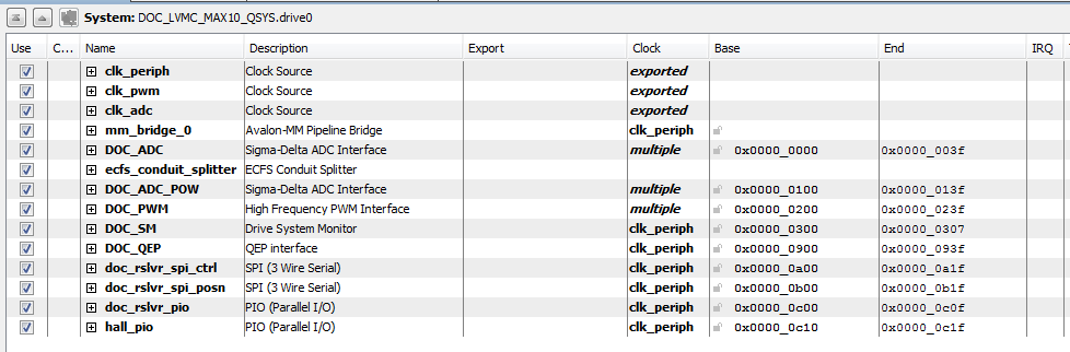
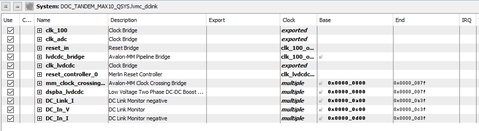
Figure 24. Qsys System for DC-DC Converter